Wafer Level Packaging Market Size, Share, Trends and Forecast by Packaging Technology, End Use Industry, and Region, 2025-2033
Wafer Level Packaging Market Size and Share:
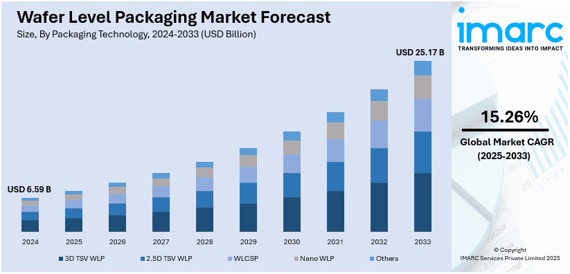
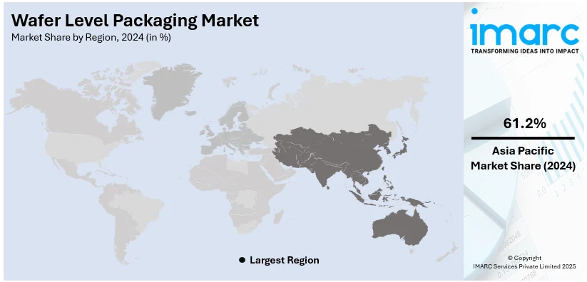
The global wafer level packaging market size was valued at USD 6.59 Billion in 2024. Looking forward, IMARC Group estimates the market to reach USD 25.17 Billion by 2033, exhibiting a CAGR of 15.26% during 2025-2033 Asia-Pacific currently dominates the market, holding a significant market share of over 61.2% in 2024. The Asia Pacific wafer level packaging market share is fueled by the region's fast-paced technological growth, increasing demand for compact and efficient electronic devices, and the growth of semiconductor production. Rising investments in 5G, IoT, and automotive electronics also drive the market growth, encouraging innovative packaging solutions.
|
Report Attribute
|
Key Statistics
|
|---|---|
|
Base Year
|
2024
|
|
Forecast Years
|
2025-2033
|
|
Historical Years
|
2019-2024
|
|
Market Size in 2024
|
USD 6.59 Billion |
|
Market Forecast in 2033
|
USD 25.17 Billion |
| Market Growth Rate 2025-2033 | 15.26% |
The wafer level packaging market outlook is driven by the demand for miniaturized, high-performance, and efficient electronic devices. As consumer electronics like smartphones, wearables, and IoT products reduce in size but need higher features, WLP provides a solution by facilitating small and high-density packaging. The growing need for miniaturization and greater functionality is driving the use of WLP technology. Also, markets such as automotive electronics, 5G, and data centers are fueling growth in the market because these markets require more sophisticated chips with faster processing. WLP facilitates higher performance, improved thermal management, and reduced power consumption, which is ideal for future use. Besides this, the pressure to reduce costs and efficient production is forcing vendors to shift towards WLP because of its lower cost of manufacturing compared to traditional packaging. The requirement for advanced packaging solutions, in combination with technological advancements, will also continue to enhance the development of the WLP market.
The United States stands out as a key market disruptor, driven by its leadership in semiconductor manufacturing, innovation, and technology development. Being a technology company hub for the entire world, the US propels demand for leading-edge packaging solutions for high-performance end markets like smartphones, 5G, artificial intelligence, and automotive electronics. High research and development investments by the country and its presence of big semiconductor players, such as Intel and Qualcomm, ensure ongoing innovation with WLP technology. In addition, increased penetration of compact and efficient devices across various industries fuels demand for WLP solutions that support miniaturization, increased functionality, and better chip performance. The United States is also a key driver in building 5G infrastructure that needs state-of-the-art packaging solutions to address the needs of high-speed communication networks. As advancements in technology advance further, the US market will guide the wafer level packaging business worldwide, determine trends for the industry, and drive the market to develop even further.
Wafer Level Packaging Market Trends:
Growth in the Electronics Industry
A significant trend in the wafer level packaging (WLP) market is the rapid growth of the global electronics industry, which is driving the demand for advanced packaging solutions. As consumer electronics such as smartphones, wearables, and IoT devices continue to evolve, the need for smaller, lighter, and more efficient chips has become critical. The International Labour Organization 2024 report highlights the electronics industry as one of the world’s largest and fastest-growing sectors, valued at EUR 1.5 Trillion and expanding at 4% annually. In 2023, it provided 17.4 Million direct jobs, with indirect employment supporting Millions more along the supply chain. WLP technology enables compact and high-performance devices by reducing the size of packaging while improving functionality and reliability. Additionally, sectors such as automotive electronics, healthcare, and industrial automation are increasingly relying on advanced semiconductor solutions, further fueling the demand for WLP. The global surge in demand for electronic devices, driven by increasing connectivity, smart devices, and technological advancements, is accelerating the adoption of wafer level packaging in various applications, ensuring its pivotal role in meeting the needs of the electronics market.
Technological Advancements
Another key trend is the continuous technological advancements in wafer level packaging, aimed at enhancing performance and cost-efficiency. Innovations such as advanced materials, 3D packaging, and heterogeneous integration are improving the functionality and thermal management of WLP solutions. Additionally, various technological advancements, such as the integration of connected devices with the Internet of Things (IoT), are acting as other growth-inducing factors. According to reports, 16.6 Billion IoT devices were connected by end-2023 (15% growth from 2022), expected to rise 13% to 18.8 Billion in 2024. 51% of enterprises plan to increase IoT budgets, with 22% expecting a 10%+ rise over 2023 levels. Apart from this, the adoption of finer pitch designs, enhanced interconnects, and more precise manufacturing techniques is also allowing for the production of more powerful, energy-efficient, and reliable semiconductor components. Improvements in packaging technology, including fan-out wafer level packaging (FOWLP) and system-in-package (SiP) solutions, are facilitating the combination of various functions into one package. Additional factors, such as the growing miniaturization of circuits in microelectronic devices and significant research and development (R&D) efforts, are expected to further propel the wafer level packaging demand.
Rising Usage of Wafer-Level Packaging in Automotive and 5G Solutions
Growing usage of wafer-level packaging (WLP) in the automotive industry, especially with electric vehicles (EVs) and autonomous driving solutions, and also in 5G technology are other major trends in the market for wafer-level packaging. According to the IMARC Group, the global 5G infrastructure market size was valued at USD 14.81 Billion in 2024 and is further expected to reach USD 368.85 Billion by 2033. Automotive applications require highly reliable and rugged semiconductor devices that can be used in rugged environments without degradation in performance and hence WLP is an apt packaging solution for such applications. WLP enables the integration of several components in a small package, which is essential for the miniaturization and lightening of electronic systems applied in vehicles. Moreover, with the automotive sector embracing more sophisticated technologies, such as sensor systems for autonomous driving, the demand for effective, high-performance packaging solutions such as WLP rises. In the 5G arena, WLP facilitates smaller, more efficient devices that are critical to the faster data transfer and reduced latency needed in next-generation networks. This is likely to continue as WLP addresses the increasing needs of both automotive and 5G applications, driving the market's growth.
Wafer Level Packaging Industry Segmentation:
IMARC Group provides an analysis of the key trends in each segment of the global wafer level packaging market, along with forecasts at the global, regional, and country levels from 2025-2033. The market has been categorized based on packaging technology and end use industry.
Analysis by Packaging Technology:
- 3D TSV WLP
- 2.5D TSV WLP
- WLCSP
- Nano WLP
- Others
2.5D TSV WLP stands as the largest component in 2024, holding around 37.1% of the market. 2.5D Through-Silicon Via (TSV) wafer level packaging (WLP) is one of the major packaging technology segments in the world's WLP market owing to its potential for supporting high-performance, high-density semiconductor devices. As compared to conventional packaging techniques, 2.5D TSV supports the integration of several chips on a common substrate, resulting in enhanced performance and lower space demands. This technology relies on vertical interconnects along the silicon wafer, with a bridge built between stacked chips to facilitate fast communication and minimizing signal loss. The use of 2.5D TSV is due to the increase in demand for miniaturization and increased processing power in telecommunications, consumer electronics, and automobiles. With uses like high-performance computing, gaming hardware, and 5G equipment, 2.5D TSV has the benefits of bandwidth, power consumption, and space savings. The demand for quicker, more capable devices keeps fueling the requirement for this technology, making 2.5D TSV a central facilitator of the future generation of semiconductors.
Analysis by End Use Industry:
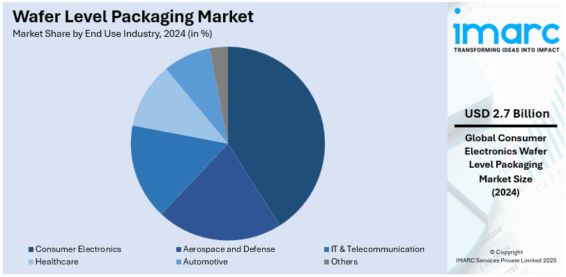
- Aerospace and Defense
- Consumer Electronics
- IT & Telecommunication
- Healthcare
- Automotive
- Others
Consumer electronics leads the market with around 40.3% of market share in 2024. Consumer electronics is the most prominent end-use industry segment fueling the wafer level packaging (WLP) market. As electronic devices become smaller, faster, and more efficient, WLP technology has become vital to meet these demands. Smartphones, wearables, tablets, and other portable electronics are becoming smaller in size while being larger in functionality, and thus sophisticated packaging solutions such as WLP are becoming increasingly important. WLP provides a number of benefits such as increased integration, improved thermal efficiency, and superior performance, all with less packaging size. This makes it perfectly suitable for environments where space is restricted and performance is paramount. The consumer electronics market, fueled by technology advancements like 5G smartphones, smart home appliances, and future-generation wearables, continues to drive miniaturization, placing a high demand for WLP solutions. Further, with a focus on miniaturized, more powerful consumer goods, there has been rising acceptance of WLP by makers in order to offer high-tech, high-performing products. Hence, the consumer electronics segment is still the single largest stimulus behind the overall world WLP market.
Regional Analysis:
- North America
- United States
- Canada
- Asia-Pacific
- China
- Japan
- India
- South Korea
- Australia
- Indonesia
- Others
- Europe
- Germany
- France
- United Kingdom
- Italy
- Spain
- Russia
- Others
- Latin America
- Brazil
- Mexico
- Others
- Middle East and Africa
In 2024, Asia-Pacific accounted for the largest market share of over 61.2%. Asia Pacific wafer level packaging (WLP) market is led by fast-paced technological developments and an increased need for compact, efficient electronic products. With the presence of leading semiconductor companies in the region, including Taiwan, South Korea, and Japan, the use of WLP technology has picked up pace. WLP facilitates the creation of smaller and more integrated products, which is paramount as businesses transition toward miniaturization for consumer electronics, smartphones, and wearables. Further, the growing demand for high-performance chips in applications such as 5G, IoT, and automotive electronics is compounding the requirement for sophisticated packaging solutions that WLP can offer. The high research and development investments as well as robust manufacturing capabilities of the Asia Pacific region are also contributing to the growing use of wafer level packaging. Additionally, the transition to high-density interconnects, enhanced signal integrity, and cost-saving offerings makes WLP appealing, leading to its extensive usage among the region's numerous industries.
Key Regional Takeaways:
United States Wafer Level Packaging Market Analysis
In 2024, the United States accounted for over 89.50% of the wafer level packaging market in North America. The United States wafer level packaging market is growing, fueled by AI, high-performance computing (HPC), and 5G technologies. Likewise, leading companies are making significant investments in advanced semiconductor packaging to improve chip performance, power efficiency, and integration. The CHIPS and Science Act is speeding up domestic semiconductor manufacturing, increasing demand for wafer-level fan-out (WLFO) and fan-in (WLFI) packaging. In addition, the expanding popularity of chiplet-based architectures used in AI as well as in data centers is driving 2.5D and 3D WLP usage, advancing connectivity and heat management in applications with high performance. The auto industry is likewise a leading market driver of demand for WLP, with rapid growth in the adoption of EVs and autonomous vehicles. In 3Q24, hybrid and electric vehicles accounted for an all-time 21.2% of LDV sales, up from 19.1% during 2Q24, states the U.S. EIA. Battery electric vehicles (BEVs) propelled the increase with 7.4% going to 8.9%, and hybrid units recorded 10.6% at a record level. Apart from this, the automotive manufacturers are including advanced driver assistance systems (ADAS) and vehicle computing, leading to a need for high-density semiconductor packaging that provides reliability, miniaturization, and high processing capability. All these trends make WLP a key technology for future automotive, AI, and telecom applications in the market.
Europe Wafer Level Packaging Market Analysis
The wafer level packaging market in Europe is expanding due to automotive electrification, industrial automation, and IoT growth. For instance, in December 2024, the European Investment Bank (EIB) granted EUR 30 Million to Sateliot to expand its NB-IoT satellite constellation, strengthening global IoT connectivity in remote areas. Sateliot targets EUR 1 Billion revenue by 2030, with four LEO satellites launching commercial services in 2025. Furthermore, Germany, France, and the Netherlands lead the sector, benefiting from strong semiconductor research institutions and collaborations between automotive and semiconductor companies. The European Chips Act is accelerating semiconductor independence, increasing investments in advanced wafer-level packaging (WLP) for AI applications, autonomous vehicles, and high-performance computing (HPC). The demand for fan-out wafer-level packaging (FOWLP) is increasing in automotive, consumer electronics, and healthcare, as companies seek high-reliability, compact, and cost-efficient solutions. Additionally, the ongoing shift toward heterogeneous integration is particularly strong in photonics and MEMS packaging, with European firms focusing on optical communication technologies. Besides this, strict environmental regulations drive eco-friendly packaging and energy-efficient production, making WLP essential for Europe’s semiconductor sustainability initiatives. The focus on energy efficiency and electronic waste reduction pushes low-power chip packaging innovation, aligning with EU climate goals and supporting sustainable electronics manufacturing.
Asia Pacific Wafer Level Packaging Market Analysis
The Asia Pacific market leads globally, driven by semiconductor giants in China, Taiwan, South Korea, and Japan. In line with this, these companies pioneer innovations in wafer-level chip-scale packaging (WLCSP), fan-out wafer-level packaging (FOWLP), and hybrid bonding, essential for AI, 5G, and high-performance computing (HPC). The rise of local semiconductor supply chains in India and Southeast Asia is fostering WLP adoption, especially in consumer electronics and automotive applications. Furthermore, the booming smartphone market in China and India increases demand for compact, high-performance chip packaging, aligning with miniaturization trends. According to data, China's smartphone market shipped 76.4 Million units in 4Q24, up 3.9% YoY, driven by new launches and government subsidies. Full-year 2024 shipments reached 286.2 Million units, growing 5.6% YoY, marking a recovery after two years of decline. The expansion of foundry services and panel-level packaging (PLP) investments in South Korea and Taiwan drive further innovation. Besides this, China and India’s government initiatives aim to reduce semiconductor dependency, augmenting local production.
Latin America Wafer Level Packaging Market Analysis
The wafer level packaging market in Latin America is growing, propelled by consumer electronics, telecommunications, and automotive demand. Brazil and Mexico lead the region, benefiting from investments in electronic manufacturing services (EMS) and automotive semiconductor production. Similarly, 5G expansion is fueling high-performance chip packaging, supporting wireless communication and IoT assembly plants. According to GSMA, Latin America’s 5G adoption is 5% of total connections, expected to reach 14% by 2025, with Argentina, Brazil, Chile, Mexico, Guatemala, and Uruguay seeing double-digit shares. Moreover, Mexico’s strong electronics manufacturing base is attracting foreign investments in fan-out and wafer-level chip-scale packaging for mobile and wearables. While Latin America lacks major semiconductor fabs, partnerships with the U.S. and Europe are driving WLP adoption in data centers, smart cities, and electric vehicles, fostering regional semiconductor development.
Middle East and Africa Wafer Level Packaging Market Analysis
The market in Middle East and Africa is growing given investments in AI, data centers, and 5G networks. For example, in November 2024, Saudi Arabia launched Project Transcendence, a USD 100 Billion AI initiative focusing on data centers, AI startups, and workforce development. Google, investing USD 5-10 Billion, is developing Arabic-language AI models. Saudi Vision 2030 and the UAE’s National Innovation Strategy promote semiconductor research and local chip assembly. Apart from this, South Africa’s continual advancements in automotive electronics and industrial automation further support demand. Though local semiconductor production remains limited, MEA attracts investments in testing and assembly, with WLP solutions expanding in telecommunications, renewable energy, and medical applications to support economic diversification and technological self-sufficiency.
Competitive Landscape:
Several major companies in the wafer level packaging (WLP) market are adopting some strategic initiatives to fuel growth and accommodate the rising demand for sophisticated semiconductor solutions. Large corporations are investing in ongoing innovation in packaging technologies, including the creation of fan-out wafer level packaging (FOWLP) and system-in-package (SiP) solutions. These technologies allow for greater integration, better performance, and smaller size, which makes them well-suited for consumer electronics, telecommunications, and automotive applications. In order to address the increasing demand for miniaturization and increased functionality, these firms are also spending on research and development to improve the thermal management and power efficiency of WLP solutions. In addition, market leaders are streamlining their production process to decrease cost and enhance scalability, which makes wafer level packaging affordable to a wide array of industries. Collaboration and partnership between semiconductor manufacturers, packaging service providers, and technology companies are also another significant approach, which facilitates the creation of new and affordable packaging solutions. In addition, leading industry players are also ramping up their manufacturing presence in the Asia Pacific region as demand for sophisticated packaging is increasing rapidly with the growth of the electronics and automotive sectors. By doing so, leading players are positioning themselves to take advantage of the emerging WLP market and drive the global trend toward smaller, lower-power electronic devices.
The report provides a comprehensive analysis of the competitive landscape in the wafer level packaging market with detailed profiles of all major companies, including:
- Amkor Technology Inc.
- China Wafer Level CSP Co. Ltd.
- Chipbond Technology Corporation
- Deca Technologies Inc. (Infineon Technologies AG)
- Fujitsu Limited
- IQE PLC
- JCET Group Co. Ltd.
- Siliconware Precision Industries Co. Ltd. (Advanced Semiconductor Engineering Inc.)
- Tokyo Electron Ltd.
- Toshiba Corporation
Latest News and Developments:
- February 2025: LQDX Inc. signed an agreement with Arizona State University (ASU) to advance IC-substrates and wafer-level packaging using Liquid Metal Ink (LMI) technology. ASU’s Advanced Packaging Piloting Facility will support research under the CHIPS for America initiative, strengthening US semiconductor packaging innovation within Arizona’s growing ecosystem.
- January 2025: Yield Engineering Systems (YES) announced multiple VertaCure PLP system orders from a leading Japanese semiconductor manufacturer for AI and HPC solutions. The automated vacuum curing system supports 2.5D/3D packaging and wafer-level packaging, ensuring superior film performance, precise temperature control, and enhanced polymer curing for Polyimide, PBO, and build-up layers, essential for advanced semiconductor manufacturing.
- January 2025: The 2025 Wafer-Level Packaging Symposium, hosted by SMTA, will take place February 18-20, 2025, in San Francisco. Featuring 20+ expert speakers, it includes a keynote by Nvidia and the Semiconductor Industry Association on the CHIPS Act and sessions on packaging advances, AI, and HPC challenges.
- October 2024: DELO introduced a UV-curing approach for fan-out wafer-level packaging (FOWLP), reducing warpage, die shift, curing time, and energy consumption. Unlike heat-curing methods, UV-curable materials minimize thermal expansion mismatch and allow low-viscosity molding without high pressure or heat.
- August 2024: Nordson Electronics Solutions announced its high-throughput fluid dispensing technologies for wafer-level and panel-level packaging at SEMICON Taiwan 2024 (booth L0516). Featuring the ASYMTEK Forte and Vantage systems, these solutions enhance precision and efficiency in semiconductor packaging while addressing warpage challenges in high-volume manufacturing.
Wafer Level Packaging Market Report Coverage:
| Report Features | Details |
|---|---|
| Base Year of the Analysis | 2024 |
| Historical Period | 2019-2024 |
| Forecast Period | 2025-2033 |
| Units | Billion USD |
| Scope of the Report |
Exploration of Historical Trends and Market Outlook, Industry Catalysts and Challenges, Segment-Wise Historical and Future Market Assessment:
|
| Packaging Technologies Covered | 3D TSV WLP, 2.5D TSV WLP, WLCSP, Nano WLP, Others |
| End Use Industries Covered | Aerospace and Defense, Consumer Electronics, IT & Telecommunication, Healthcare, Automotive, Others |
| Region Covered | Asia Pacific, Europe, North America, Latin America, Middle East and Africa |
| Countries Covered | United States, Canada, Germany, France, United Kingdom, Italy, Spain, Russia, China, Japan, India, South Korea, Australia, Indonesia, Brazil, Mexico |
| Companies Covered | Amkor Technology Inc., China Wafer Level CSP Co. Ltd., Chipbond Technology Corporation, Deca Technologies Inc. (Infineon Technologies AG), Fujitsu Limited, IQE PLC, JCET Group Co. Ltd., Siliconware Precision Industries Co. Ltd. (Advanced Semiconductor Engineering Inc.), Tokyo Electron Ltd., Toshiba Corporation, etc. |
| Customization Scope | 10% Free Customization |
| Post-Sale Analyst Support | 10-12 Weeks |
| Delivery Format | PDF and Excel through Email (We can also provide the editable version of the report in PPT/Word format on special request) |
Key Benefits for Stakeholders:
- IMARC’s report offers a comprehensive quantitative analysis of various market segments, historical and current market trends, market forecasts, and dynamics of the wafer level packaging market from 2019-2033.
- The research study provides the latest information on the market drivers, challenges, and opportunities in the global wafer level packaging market.
- The study maps the leading, as well as the fastest-growing, regional markets. It further enables stakeholders to identify the key country-level markets within each region.
- Porter's Five Forces analysis assists stakeholders in assessing the impact of new entrants, competitive rivalry, supplier power, buyer power, and the threat of substitution. It helps stakeholders to analyze the level of competition within the wafer level packaging industry and its attractiveness.
- Competitive landscape allows stakeholders to understand their competitive environment and provides an insight into the current positions of key players in the market.
Key Questions Answered in This Report
The wafer level packaging market was valued at USD 6.59 Billion in 2024.
The wafer level packaging market is projected to exhibit a CAGR of 15.26% during 2025-2033, reaching a value of USD 25.17 Billion by 2033.
The wafer level packaging market is driven by the demand for smaller, more efficient electronic devices, increasing miniaturization in consumer electronics, and the need for high-performance semiconductors. Technological advancements, such as 3D packaging and improved thermal management, further boost the adoption of wafer level packaging across various industries.
Asia Pacific currently dominates the wafer level packaging market, accounting for a share of 61.2%. The Asia Pacific wafer level packaging market is driven by rapid technological advancements, the region’s dominance in semiconductor manufacturing, and the increasing demand for compact, high-performance electronic devices. Rising investments in 5G, IoT, and automotive electronics further fuel the market, promoting the need for advanced packaging solutions.
Some of the major players in the wafer level packaging market include Amkor Technology Inc., China Wafer Level CSP Co. Ltd., Chipbond Technology Corporation, Deca Technologies Inc. (Infineon Technologies AG), Fujitsu Limited, IQE PLC, JCET Group Co. Ltd., Siliconware Precision Industries Co. Ltd. (Advanced Semiconductor Engineering Inc.), Tokyo Electron Ltd., Toshiba Corporation, etc.
Need more help?
- Speak to our experienced analysts for insights on the current market scenarios.
- Include additional segments and countries to customize the report as per your requirement.
- Gain an unparalleled competitive advantage in your domain by understanding how to utilize the report and positively impacting your operations and revenue.
- For further assistance, please connect with our analysts.
 Request Customization
 Speak to an Analyst
 Request Brochure
 Inquire Before Buying
Benefits of Customization
- Personalize this research
- Triangulate with your data
- Get data as per your format and definition
- Gain a deeper dive into a specific application, geography, customer, or competitor
- Any level of personalization
Get in Touch With Us
UNITED STATES
Phone: +1-201-971-6302
INDIA
Phone: +91-120-433-0800
UNITED KINGDOM
Phone: +44-753-714-6104
Email: sales@imarcgroup.com
Client Testimonials
.webp)