
United States Semiconductor Manufacturing Equipment Market Size, Share, Trends and Forecast by Equipment Type, Product Type, Dimension, Supply Chain Participant, and Region, 2026-2034
United States Semiconductor Manufacturing Equipment Market Size, Share, Trends & Forecast (2026-2034)
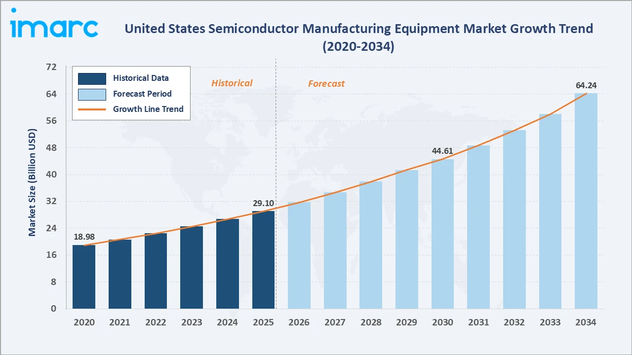
The United States semiconductor manufacturing equipment market grew from USD 29.10 Billion in 2025 to USD 31.70 Billion in 2026 and is projected to reach USD 64.24 Billion by 2034, growing at a CAGR of 8.92% during 2026-2034. The market is propelled by robust government investments under the CHIPS and Science Act, surging demand for AI and data center chips, and rapid expansion of domestic semiconductor fabrication capacity.
Expanding domestic fab construction, AI infrastructure semiconductor demand, and growing defense chip self-sufficiency requirements are further supporting market growth. Logic components dominate at 28.7%. The 2D dimension segment commands 62.3%. The West region holds 34.6% of national market share.
Market Snapshot
|
Metric |
Value |
|
Base Year Market Size (2025) |
USD 29.10 Billion |
|
Market Size (2026) |
USD 31.70 Billion |
|
Forecast Market Size (2034) |
USD 64.24 Billion |
|
CAGR (2026-2034) |
8.92% |
|
Base Year |
2025 |
|
Historical Period |
2020-2025 |
|
Forecast Period |
2026-2034 |
|
Dominant Product Type |
Logic Components (28.7%, 2025) |
|
Dominant Dimension |
2D (62.3%, 2025) |
|
Leading Region |
West (34.6%, 2025) |
The U.S. semiconductor manufacturing equipment market size increased from USD 18.98 Billion in 2020 to USD 29.10 Billion in 2025 and is estimated to reach USD 31.70 Billion in 2026. The market is further expected to grow to USD 44.61 Billion by 2030 and USD 64.24 Billion by 2034.
To get more information on this market, Request Sample
The U.S. semiconductor manufacturing equipment market is projected to grow at a CAGR of 8.92% during 2026–2034, driven by advanced-node fab expansion, AI chip demand, and domestic semiconductor manufacturing capacity buildout under the CHIPS and Science Act.
Executive Summary
The U.S. semiconductor manufacturing equipment market expanded from USD 29.10 Billion in 2025 to an estimated USD 31.70 Billion in 2026, positioning the U.S. as the world's leading hub for advanced semiconductor production infrastructure. The market is projected to reach USD 64.24 Billion by 2034. Logic components at 28.7% lead product type share. The 2D dimension at 62.3% underpins mainstream fab processes. The West region commands 34.6%.
Key Market Insights
|
Insight |
Data |
|
Dominant Product Type |
Logic Components – 28.7% share (2025) |
|
Dominant Dimension |
2D – 62.3% market share (2025) |
|
Leading Region |
West – 34.6% share (2025) |
|
Market Opportunity |
CHIPS Act fab buildout; AI chip demand; advanced packaging expansion |
Key Analytical Observations Supporting the Above Data:
- Logic Components at 28.7%: The logic segment dominates due to accelerating demand for AI accelerators, GPUs, and CPUs that require the highest equipment intensity per wafer. U.S. fabs at advanced nodes below 7 nm are primarily logic-oriented, driving outsized front-end equipment procurement for lithography, deposition, and etch tools that represent the highest-value equipment categories in the market.
- 2D at 62.3%: Conventional planar semiconductor manufacturing retains majority volume share as mainstream and legacy nodes constitute the bulk of production capacity across U.S. fabs serving automotive, industrial, and consumer electronics markets where 2D processes remain economically optimal for the device performance and cost requirements of the target applications.
- West at 34.6%: The West region leads through California's semiconductor equipment OEM headquarters concentration, Oregon's Intel logic manufacturing scale, and Arizona's TSMC advanced-node fab ramp, creating the highest regional equipment procurement density and process innovation activity across the entire U.S. semiconductor manufacturing ecosystem.
United States Semiconductor Manufacturing Equipment Market Overview
The U.S. semiconductor manufacturing equipment market occupies a unique commercial and strategic position: the world's leading technology economy with deep private-sector semiconductor R&D, a mature IDM and foundry ecosystem, and accelerating government investment in domestic chip sovereignty under the CHIPS and Science Act. This combination creates a structurally favorable equipment demand environment that distinguishes the U.S. from all other national semiconductor markets.
Market Dynamics
To evaluate market opportunities, Request Sample
Market Drivers
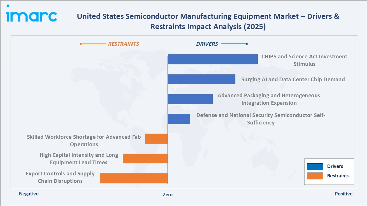
- CHIPS and Science Act Investment Stimulus: The CHIPS and Science Act has unlocked over USD 52 billion in federal subsidies for domestic semiconductor manufacturing, directly increasing capital equipment demand across lithography, deposition, etch, and metrology categories. New fab construction by Intel in Ohio, TSMC in Arizona, and Samsung in Texas accelerates multi-year structured equipment procurement cycles that underpin market growth well into 2034. These federally incentivized investments are creating the largest single expansion of U.S. semiconductor manufacturing capacity since the 1990s, with equipment procurement timelines spanning 2025 through 2030 as fabs progress from construction to full production ramp. CHIPS Act direct grants and investment tax credits are materially reducing the cost of capital for participating chipmakers, enabling larger and faster equipment procurement commitments than private financing alone would support.
- Surging AI and Data Center Chip Demand: Exponential growth in AI model training and inference workloads is driving unprecedented demand for advanced logic semiconductors, including GPUs, AI accelerators, and custom silicon from hyperscalers. This demand cycle is structurally different from prior semiconductor cycles because AI infrastructure investment is driven by competitive necessity among hyperscalers rather than consumer electronics cycles, creating more durable and less cyclical equipment demand. The shift to custom AI accelerator chips from merchant silicon is increasing the number of advanced-node fab customers, diversifying equipment procurement across multiple chipmakers.
- Advanced Packaging and Heterogeneous Integration Expansion: Chipmakers are adopting advanced packaging including 2.5D interposers, CoWoS, and 3D stacking to achieve performance gains beyond node shrinks, driving demand for bonding, wafer-level packaging, and metrology equipment. The transition to chiplet architectures is creating entirely new equipment categories for advanced packaging inspection, die-to-wafer bonding, and hybrid bonding that were not significant market segments five years ago, representing the fastest-growing equipment investment category in the U.S. market through 2034.
- Defense and National Security Semiconductor Self-Sufficiency: The U.S. Department of Defense is prioritizing domestic semiconductor production for military-grade chips through programs including the Microelectronics Commons, DARPA electronics initiatives, and secure fab designations. These programs sustain demand for specialty process equipment including compound semiconductor tools, radiation-hardened chip production lines, and secure domestic fabrication infrastructure above commercial demand cycles. Defense semiconductor requirements create a structurally non-cyclical equipment demand segment that persists regardless of commercial semiconductor market cycles, providing equipment suppliers with a stable government-funded revenue base across all market conditions.
Market Restraints
- Export Controls and Supply Chain Disruptions: U.S. export controls on advanced semiconductor equipment to China have restricted revenue for U.S.-headquartered equipment suppliers, affecting sales of EUV, advanced etch, and deposition systems to Chinese fabs. These restrictions reduce the total addressable market for equipment suppliers and create pricing pressure in non-restricted geographies as displaced Chinese demand competes for alternative markets at below-ceiling pricing. The Bureau of Industry and Security's expanding equipment export control list creates ongoing uncertainty for equipment supplier revenue planning, as additional tool categories may face export restrictions without advance warning, increasing operational costs and reducing the economic efficiency of global product development programs.
- High Capital Intensity and Long Equipment Lead Times: Advanced semiconductor manufacturing equipment, particularly EUV lithography systems and multi-chamber deposition tools, requires extensive capital commitment with per-tool costs exceeding USD 150 million for leading-edge systems. Extended lead times of 12–18 months constrain rapid capacity response, potentially slowing revenue realization for equipment suppliers despite strong order books during periods of rapid fab expansion. The capital intensity of advanced equipment creates a concentrated supplier structure in leading-edge categories, limiting competitive dynamics that would otherwise drive equipment cost reduction and sustaining high equipment prices that increase fab investment requirements above pure technology cost curves.
- Skilled Workforce Shortage for Advanced Fab Operations: The rapid expansion of domestic semiconductor fabs is constrained by a shortage of trained semiconductor process engineers and equipment technicians. Workforce gaps slow fab ramp-up timelines, reduce equipment utilization efficiency, and suppress full demand conversion from fab construction commitments into active equipment procurement and production ramp. The semiconductor workforce shortage is most acute in specialized equipment process engineering roles that require years of on-tool experience at specific nodes to develop competency, and domestic universities are not producing semiconductor engineers at the pace required to staff CHIPS Act-funded fab expansions.
Market Opportunities
- Advanced Node Lithography Expansion for 2 nm and Below: Transition to 2 nm and gate-all-around transistor architectures requires entirely new equipment generations including High-NA EUV lithography, new dry resist systems, and advanced process control tools, creating replacement demand cycles above capacity expansion. This technology transition generates additional equipment revenue at Intel, TSMC Arizona, and Samsung as each node transition requires significant new tool investment per wafer start.
- Silicon Carbide and Compound Semiconductor Equipment Demand: Electric vehicle adoption and power electronics demand are accelerating SiC and GaN semiconductor production in the U.S., requiring specialized epitaxy, ion implantation, and packaging equipment that serves a rapidly growing adjacent market beyond conventional silicon. Multiple domestic SiC fab expansions by leading manufacturers are creating structured equipment procurement cycles that diversify equipment supplier revenue above the leading-edge silicon equipment market.
Market Challenges
- Rapid Technology Obsolescence and R&D Investment Pressure: Rapid technology transitions at advanced semiconductor nodes are compressing equipment lifecycle windows, requiring equipment suppliers to invest continuously in next-generation tool development while managing the commercial risk of reduced installed base longevity. Consumers and fab customers expect continuous equipment performance improvements across yield, throughput, and process control that make prior-generation tools commercially uncompetitive within 3–5 years of introduction.
- Geopolitical Uncertainty and Supply Chain Concentration Risk: Geopolitical tensions between the U.S. and China create structural uncertainty for semiconductor equipment supply chains that are deeply integrated across multiple nations for specialized components including optics, precision mechanics, and specialty materials. Equipment suppliers face growing pressure to regionalize supply chains for national security compliance, increasing manufacturing costs and reducing the global optimization that has historically driven equipment cost reduction and performance improvement.
Emerging Market Trends
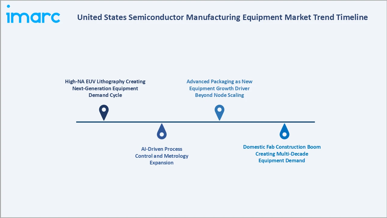
1. High-NA EUV Lithography Creating Next-Generation Equipment Demand Cycle
High-NA EUV systems with numerical aperture of 0.55 versus 0.33 for current EUV enable sub-2 nm patterning and represent the industry's most commercially impactful equipment transition. U.S. fabs are investing in High-NA EUV qualification, creating outsized tool procurement spend per wafer start at leading-edge nodes. This technology shift is expected to drive a new equipment investment cycle through 2030 as 2 nm and gate-all-around production scales across domestic fabs in Arizona, Oregon, and Ohio, representing the largest single equipment-driven revenue growth opportunity in the market.
2. AI-Driven Process Control and Metrology Expansion
AI-integrated process control tools are enabling real-time defect detection, yield optimization, and equipment predictive maintenance at leading-edge nodes where traditional statistical process control is insufficient for the density of required inspection steps.
3. Domestic Fab Construction Boom Creating Multi-Decade Equipment Demand
TSMC Arizona, Intel Ohio, Samsung Texas, and Micron Idaho represent over USD 400 billion in domestic fab investment commitments through 2030, creating staggered, highly predictable equipment procurement waves across lithography, deposition, etch, and packaging tool categories. These construction and ramp timelines provide equipment suppliers with multi-year order visibility that supports capacity planning, R&D investment, and workforce expansion above what prior demand cycles enabled.
4. Advanced Packaging as New Equipment Growth Driver Beyond Node Scaling
As transistor scaling economics diminish at advanced nodes, advanced packaging including chiplets, 2.5D interposers, and 3D stacking are driving new equipment categories into high-volume production for the first time. Packaging equipment revenue is growing fastest within the back-end segment as leading chipmakers deploy advanced packaging capacity, creating demand for bonding, inspection, and test equipment that expands the addressable market for back-end equipment suppliers well beyond conventional packaging equipment categories.
Industry Value Chain Analysis
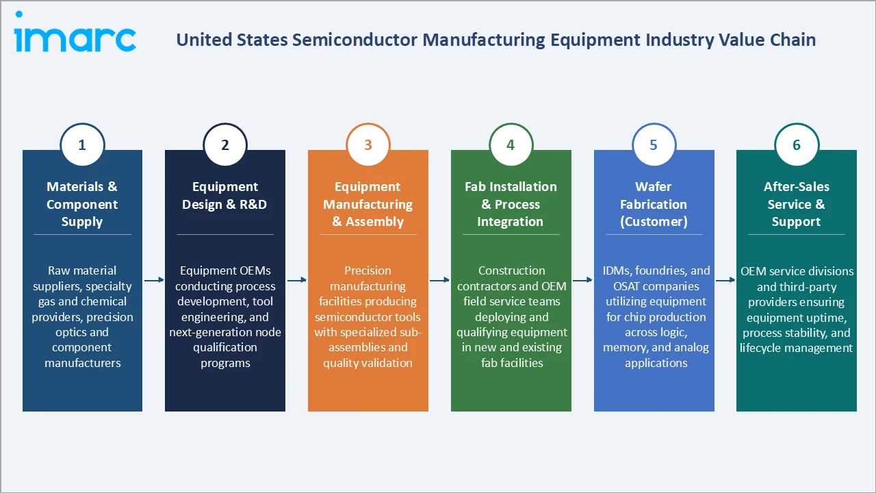
The U.S. semiconductor equipment value chain spans raw material suppliers, component manufacturers, equipment assemblers, and end-user fabs across geographically distributed but commercially integrated stages. The value chain's structure creates compounding IP advantages for U.S.-headquartered equipment suppliers, who hold dominant positions in process control, deposition, and etch categories built over decades of process development investment in close collaboration with leading chipmakers.
|
Stage |
Key Participants |
|
Materials & Component Supply |
Raw material suppliers, specialty gas and chemical providers, precision optics and component manufacturers |
|
Equipment Design & R&D |
Equipment OEMs conducting process development, tool engineering, and next-generation node qualification programs |
|
Equipment Manufacturing & Assembly |
Precision manufacturing facilities producing semiconductor tools with specialized sub-assemblies and quality validation |
|
Fab Installation & Process Integration |
Construction contractors and OEM field service teams deploying and qualifying equipment in new and existing fab facilities |
|
Wafer Fabrication (Customer) |
IDMs, foundries, and OSAT companies utilizing equipment for chip production across logic, memory, and analog applications |
|
After-Sales Service & Support |
OEM service divisions and third-party providers ensuring equipment uptime, process stability, and lifecycle management |
The equipment design and R&D stage is the most commercially consequential in the U.S. value chain, where equipment suppliers' proprietary process knowledge and application expertise create sustained competitive advantages that are difficult for new entrants to replicate. U.S. equipment OEMs co-locate R&D facilities with leading chipmakers' development fabs, enabling continuous process learning that compounds into equipment performance advantages maintained across successive node generations.
Technology Landscape in the U.S. Semiconductor Manufacturing Equipment Industry
EUV and High-NA Lithography
Extreme ultraviolet (EUV) lithography is a critical technology in advanced semiconductor manufacturing, enabling the production of increasingly smaller and more complex circuit patterns. The development of high-numerical-aperture (High-NA) EUV systems is supporting the transition toward next-generation process nodes by improving patterning precision and reducing manufacturing complexity.
Atomic Layer Deposition and Etch Technologies
Atomic layer deposition (ALD) and atomic layer etch (ALE) technologies are becoming increasingly important in advanced semiconductor manufacturing due to their ability to deliver precise material deposition and selective material removal at the atomic scale. As semiconductor manufacturers transition toward more advanced process nodes, increasing process complexity and the need for tighter fabrication tolerances are driving demand for advanced deposition and etch equipment, contributing to higher equipment requirements per production line.
AI-Integrated Process Control and Metrology
Artificial intelligence and machine learning are increasingly being integrated into semiconductor process control and metrology systems to improve defect detection, process monitoring, and manufacturing yield. AI-enabled inspection platforms and advanced measurement technologies support real-time data analysis, process optimization, and early identification of manufacturing deviations. As semiconductor fabrication becomes more complex, the growing emphasis on defect reduction, process consistency, and yield optimization is increasing demand for advanced inspection and metrology equipment, particularly in leading-edge manufacturing facilities.
Market Segmentation Analysis
The report covers the following segments:
|
Segment Category |
Leading Segment |
Market Share |
Year |
|
Equipment Type |
🔒 |
🔒 |
2025 |
|
Product Type |
Logic Components |
28.7% |
2025 |
|
Dimension |
2D |
62.3% |
2025 |
|
Supply Chain Participant |
🔒 |
🔒 |
2025 |
|
Region |
West |
34.6% |
2025 |

By Product Type
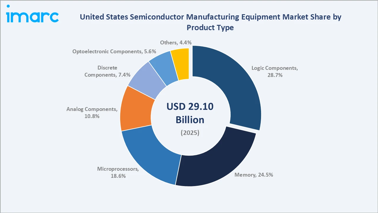
Logic components lead at 28.7% in 2025. The logic device manufacturing segment encompasses CPU, GPU, AI accelerator, and FPGA chip production, representing the highest-value semiconductor equipment investment category as hyperscalers and fabless companies drive demand for leading-edge process tools at 3 nm and below in U.S. and allied-nation fabs.
To access detailed market analysis, Request Sample
Memory at 24.5% remains the second-largest segment, driven by DRAM and NAND flash equipment demand from domestic memory manufacturing expansion and the growing importance of high-bandwidth memory for AI accelerator stacking. Microprocessors at 18.6% reflect domestic IDM and foundry production, supporting broad lithography and deposition equipment procurement at leading-edge nodes.
By Dimension
The 2D dimension segment leads at 62.3% in 2025. Conventional planar semiconductor manufacturing retains majority share as mainstream and legacy nodes constitute the bulk of production volume across U.S. fabs serving automotive, industrial, and consumer electronics markets where 2D processes remain economically optimal.
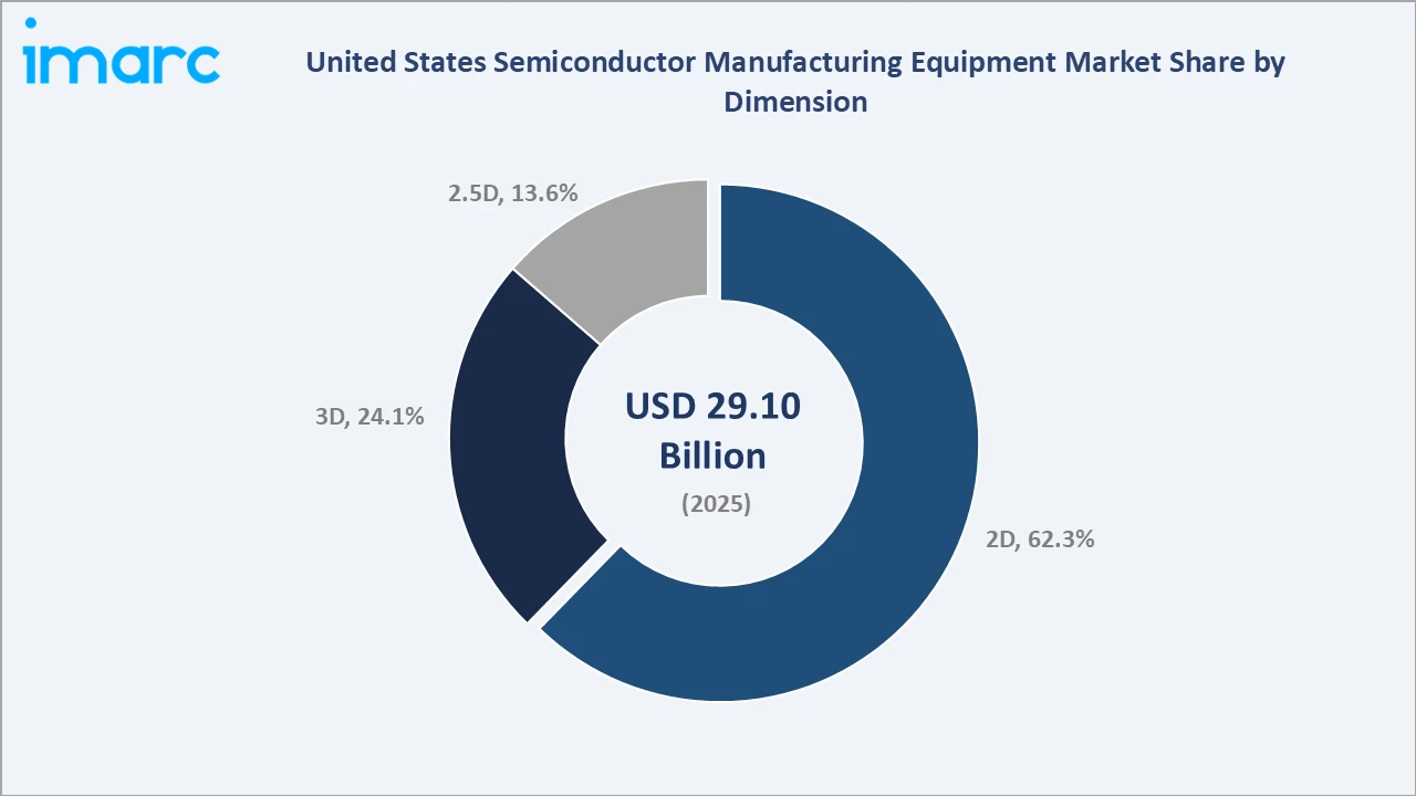
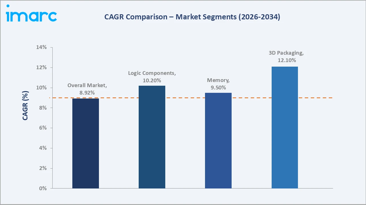
The 3D dimension segment at 24.1% is the fastest-growing dimension category at approximately 12.1% CAGR through stacked DRAM, 3D NAND expansion, and advanced 3D stacking adoption. The 2.5D segment at 13.6% is growing rapidly through CoWoS adoption for AI accelerators, with advanced packaging capacity driving 2.5D interposer equipment investment at above-market growth rates.
Regional Market Insights
|
Region |
Share (2025) |
Key Market Drivers & Characteristics |
|
West |
34.6% |
Driven by leading-edge fab concentration, equipment OEM headquarters, and high AI chip design activity generating dense equipment procurement across Arizona, Oregon, and California. |
|
South |
29.2% |
Supported by major fab investments in Texas, growing automotive and industrial semiconductor manufacturing, and robust CHIPS Act-funded construction activity across the region. |
|
Northeast |
19.4% |
Reflects domestic foundry operations, defense microelectronics manufacturing, and strong semiconductor research infrastructure across university and national laboratory networks. |
|
Midwest |
16.8% |
Driven by large-scale memory and logic fab investment, automotive chip localization initiatives, and expanding equipment installation activity aligned with multi-year domestic fab build programs. |
The West's 34.6% market leadership reflects the semiconductor equipment OEM headquarters concentration, advanced logic fab operations, and the TSMC N3E and N2 node fab ramp driving above-national equipment procurement intensity in Arizona. The South's 29.2% reflects a major foreign semiconductor investment in Texas anchoring the region alongside an extensive analog fab network and growing CHIPS Act-funded construction activity.
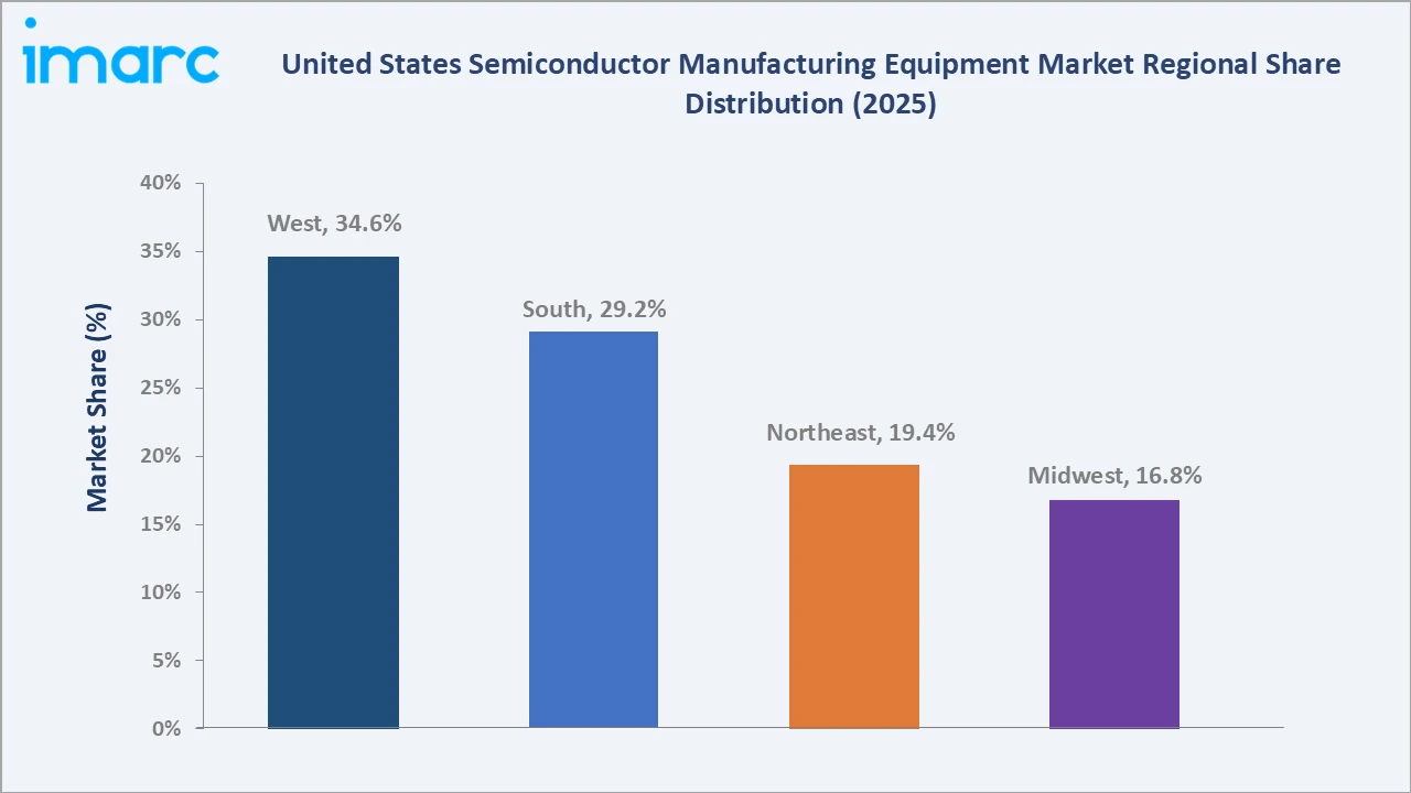
The Northeast's 19.4% share reflects domestic foundry strategic positioning for U.S. government and defense chip requirements, semiconductor research campus infrastructure, and the concentration of defense microelectronics manufacturing. The Midwest's 16.8% is transitioning rapidly as a major logic fab mega-project moves from construction to equipment installation phase through 2027, positioning the Midwest as the fastest-growing region by equipment procurement intensity through 2030.
Competitive Landscape
The U.S. semiconductor manufacturing equipment competitive landscape is globally concentrated with the top five players commanding over 70% of market revenue across their respective served equipment categories.
|
Company |
Key Products |
Market Position |
Core Strength |
|
Applied Materials, Inc. |
CVD, PVD, ALD, CMP, Etch, Metrology |
Market Leader |
Applied Materials, Inc. is the world's largest semiconductor equipment company by revenue, delivering materials engineering solutions across deposition, etch, thermal, and metrology categories for logic and memory fabs globally. |
|
Lam Research Corporation |
Etch, Deposition, Clean, Bevel |
Strong Challenger |
Lam Research Corporation dominates etch and deposition equipment with leading positions in 3D NAND and advanced logic tools, supported by a growing Customer Support Business Group providing recurring service revenue. |
|
KLA Corporation |
Inspection, Metrology, Process Control |
Innovator |
KLA Corporation leads process control and yield management with AI-driven defect inspection systems critical to maintaining yield economics at advanced nodes in domestic and allied-nation fabs. |
|
Axcelis |
Ion Implantation Systems |
Strong Challenger |
Axcelis is the leading independent ion implant equipment supplier, benefiting from SiC power device manufacturing growth and expanding U.S. domestic fab capacity buildout across logic and specialty nodes. |
|
Teradyne Inc. |
Semiconductor Test, Wafer Test |
Innovator |
Teradyne Inc. leads semiconductor test equipment with systems for memory, SoC, and automotive chips, positioned to benefit from increasing test intensity at advanced nodes and growing AI chip complexity. |
|
Onto Innovation |
Metrology, Inspection, Advanced Packaging |
Strong Challenger |
Onto Innovation Inc. provides process control and metrology solutions with growing advanced packaging inspection exposure, addressing a high-growth equipment category driven by chiplet architecture adoption. |
Key players include Applied Materials, Inc., Lam Research Corporation, KLA Corporation, Axcelis, Teradyne Inc., Onto Innovation, and others.
Key Company Profiles
Applied Materials, Inc.
Applied Materials, Inc. is the world's largest semiconductor equipment company, providing materials engineering solutions for advanced chip manufacturing across deposition, etch, thermal, CMP, and metrology categories. The company serves logic, memory, and specialty semiconductor customers with a comprehensive process equipment portfolio spanning the full wafer fabrication workflow.
- Key Products: Centura, Endura, Producer, Mirra, and Vantage platforms covering CVD, PVD, ALD, etch, CMP, and thermal processes for leading-edge logic and memory manufacturing applications.
- Strategic Focus: Expanding materials engineering platform breadth to capture incremental revenue from increasing process steps per wafer at advanced nodes, while growing services as a percentage of total revenue to reduce cyclicality and improve revenue quality through semiconductor market cycles.
Lam Research Corporation
Lam Research Corporation is a leading supplier of innovative wafer fabrication equipment and services, focused on etch, deposition, and clean technologies critical to advanced semiconductor manufacturing across logic, memory, and foundry applications. The company maintains leading market positions in 3D NAND and advanced logic process tools.
- Key Products: Kiyo etch systems, Vantex dry strip, ALTUS and SABRE deposition, and SPEED spin clean tools serving memory and logic fabs across the U.S. and allied-nation semiconductor manufacturing ecosystem.
- Strategic Focus: Deepening process tool integration with advanced-node requirements while expanding Customer Support Business Group revenue through equipment upgrades and long-term service agreements, targeting service revenue as a structural growth driver that sustains business momentum through semiconductor investment cycles.
Market Concentration Analysis
The U.S. semiconductor manufacturing equipment market is highly concentrated at the top, with the key players collectively accounting for an estimated 45–55% of domestic equipment procurement value across their served categories. The market is moderately fragmented in specialty equipment categories including ion implantation, compound semiconductor, and advanced packaging inspection tools where smaller specialized suppliers hold leading positions.
Market concentration is being reinforced by leading equipment suppliers' investment in proprietary process knowledge and AI-driven process control integration, raising switching costs for fab customers who have optimized their manufacturing processes around specific equipment platforms. Service contract structures that bundle tool qualification, process support, and upgrade rights further deepen the commercial relationship between equipment suppliers and fab customers across multi-year periods.
Investment & Growth Opportunities
Highest Growth Segments
Logic components equipment at approximately 10.2% CAGR through AI accelerator, GPU, and CPU chip production demand driving front-end equipment investment at advanced nodes, memory equipment at approximately 9.5% CAGR through DRAM and NAND flash capacity expansion, and 3D packaging equipment at approximately 12.1% CAGR through stacked memory and advanced heterogeneous integration adoption represent the highest-growth U.S. equipment investment opportunities through 2034.
Emerging Investment Opportunities
The U.S. domestic fab buildout creates structured, multi-year equipment procurement pipelines for investors seeking semiconductor capital equipment exposure with visibility into demand timing. CHIPS Act incentive structures reduce financial risk for participating fabs, indirectly de-risking equipment supplier revenue streams tied to CHIPS-funded customers. The emerging domestic compound semiconductor equipment market represents a high-growth segment that is commercially distinct from the conventional silicon equipment market.
Investment Themes
- Advanced packaging equipment investment: Capturing the fastest-growing back-end equipment segment as chiplet architectures replace monolithic chip scaling. CoWoS, HBM stacking, and 3D packaging inspection tools represent commercially addressable market expansion above the base process equipment market, with equipment suppliers positioned to grow faster than the overall market through the AI chip architecture transition.
- SiC and GaN power device equipment investment: Addressing the EV and power electronics semiconductor manufacturing boom with specialized epitaxy, ion implantation, and packaging equipment for compound semiconductor fabs. U.S. domestic SiC wafer processing equipment demand is growing at above-20% annually through 2030, creating investable equipment supplier growth well above the broader market CAGR.
Future Market Outlook (2026-2034)
The U.S. semiconductor manufacturing equipment market is projected to grow from USD 29.10 Billion in 2025 to USD 31.70 Billion in 2026, reaching USD 64.24 Billion by 2034, registering a CAGR of 8.92% during 2026–2034. The market's anchor value of approximately USD 44.61 Billion in 2030 represents the CHIPS Act fab investment cycle reaching peak equipment installation intensity, with multiple large-format domestic fabs entering active production ramp simultaneously across logic, memory, and compound semiconductor manufacturing.
Three structural forces define U.S. market growth through 2034: CHIPS Act-driven domestic fab investment creating multi-decade equipment procurement with federal cost-sharing that sustains investment above pure commercial return thresholds; AI and data center semiconductor demand driving logic and advanced packaging equipment intensity at above-historical levels; and defense chip sovereignty requirements sustaining specialty equipment demand across commercial cycle variability that provides structural floor demand for the overall equipment market.
Research Methodology
Primary Research
Primary research comprised structured interviews with semiconductor equipment industry stakeholders including Equipment Sales Directors, Fab Process Engineers, Supply Chain Managers, CHIPS Act program administrators, and defense procurement officials covering front-end equipment, back-end packaging tools, and metrology systems across U.S. fab operations spanning logic, memory, and specialty semiconductor manufacturing.
Secondary Research
Secondary research encompassed SEMI industry data, U.S. Department of Commerce semiconductor investment reports, company annual reports and investor presentations, CHIPS Act award disclosures, U.S. International Trade Commission semiconductor equipment trade data, and defense microelectronics program documentation. Over 60 primary and secondary sources were reviewed and cross-referenced for data validation.
Forecasting Models
Market revenue forecasts were developed using a fab capacity investment model: planned U.S. wafer start capacity additions multiplied by equipment intensity per technology node, aggregated across equipment categories and fab customers, with CHIPS Act funding timelines applied as investment acceleration factors. Compound semiconductor equipment forecasts used separate EV penetration and power device volume models specific to SiC and GaN manufacturing processes.
United States Semiconductor Manufacturing Equipment Market Report Coverage:
| Report Features | Details |
|---|---|
| Base Year of the Analysis | 2025 |
| Historical Period | 2020-2025 |
| Forecast Period | 2026-2034 |
| Units | Billion USD |
| Scope of the Report | Exploration of Historical Trends and Market Outlook, Industry Catalysts and Challenges, Segment-Wise Historical and Future Market Assessment:
|
| Equipment Types Covered |
|
| Product Types Covered | Memory, Logic Components, Microprocessor, Analog Components, Optoelectronic Components, Discrete Components, Others |
| Dimensions Covered | 2D, 2.5D, 3D |
| Supply Chain Participants Covered | IDM Firms, OSAT Companies, Foundries |
| Regions Covered | Northeast, Midwest, South, West |
| Companies Covered | Applied Materials, Inc., Lam Research Corporation, KLA Corporation, Axcelis, Teradyne Inc., Onto Innovation, etc. |
| Customization Scope | 10% Free Customization |
| Post-Sale Analyst Support | 10-12 Weeks |
| Delivery Format | PDF and Excel through Email (We can also provide the editable version of the report in PPT/Word format on special request) |
Key Benefits for Stakeholders:
- IMARC’s industry report offers a comprehensive quantitative analysis of various market segments, historical and current market trends, market forecasts, and dynamics of the United States semiconductor manufacturing equipment market from 2020-2034.
- The research report provides the latest information on the market drivers, challenges, and opportunities in the United States semiconductor manufacturing equipment market.
- Porter's five forces analysis assist stakeholders in assessing the impact of new entrants, competitive rivalry, supplier power, buyer power, and the threat of substitution. It helps stakeholders to analyze the level of competition within the United States semiconductor manufacturing equipment industry and its attractiveness.
- Competitive landscape allows stakeholders to understand their competitive environment and provides an insight into the current positions of key players in the market.
Frequently Asked Questions About the United States Semiconductor Manufacturing Equipment Market Report
The U.S. semiconductor manufacturing equipment market size is estimated at USD 31.70 Billion in 2026, driven by CHIPS Act-funded fab construction, AI chip demand growth, and expanded domestic semiconductor manufacturing capacity investment by Intel, TSMC, Samsung, and Micron across logic, memory, and specialty semiconductor categories.
The U.S. semiconductor manufacturing equipment market grows at a CAGR of 8.92% during 2026-2034, reaching USD 64.24 Billion by 2034. Overall growth is sustained by advanced-node fab ramp-up, AI infrastructure semiconductor demand, advanced packaging equipment adoption, and SiC and GaN compound semiconductor manufacturing expansion across domestically incentivized production facilities.
Logic components lead at 28.7% through AI accelerator, GPU, and CPU chip production demand driving front-end equipment investment in 3 nm and below process nodes. This segment is growing at approximately 10.2% CAGR, as hyperscaler AI infrastructure investment creates durable demand for advanced-node logic fab equipment through 2034.
The 2D dimension segment leads at 62.3% through conventional planar semiconductor manufacturing serving automotive, industrial, and mainstream consumer electronics markets at nodes above 10 nm. The 3D segment at 24.1% is the fastest-growing dimension category, driven by 3D NAND memory and advanced packaging stacking requirements growing rapidly as a share of total equipment procurement.
The West region leads at 34.6% through equipment OEM headquarters concentration, advanced logic fab manufacturing scale, and advanced-node fab ramp creating the highest regional equipment procurement density in the U.S. The South at 29.2% is the second-largest region, anchored by a major semiconductor fab investment in Texas and extensive analog semiconductor manufacturing infrastructure.
Leading companies include Applied Materials, Inc., Lam Research Corporation, KLA Corporation, Axcelis, Teradyne Inc., Onto Innovation, and others.
Need more help?
- Speak to our experienced analysts for insights on the current market scenarios.
- Include additional segments and countries to customize the report as per your requirement.
- Gain an unparalleled competitive advantage in your domain by understanding how to utilize the report and positively impacting your operations and revenue.
- For further assistance, please connect with our analysts.
 Request Customization
 Speak to an Analyst
 Request Brochure
 Inquire Before Buying
Benefits of Customization
- Personalize this research
- Triangulate with your data
- Get data as per your format and definition
- Gain a deeper dive into a specific application, geography, customer, or competitor
- Any level of personalization
Get in Touch With Us
UNITED STATES
Phone: +1-201-971-6302
INDIA
Phone: +91-120-433-0800
UNITED KINGDOM
Phone: +44-753-714-6104
Email: [email protected]
Client Testimonials




.webp)




.webp)












Related Reports

Choose your plan
*Please note that the prices mentioned below are starting prices for each bundle type. Kindly contact our team for further details.*
Single User License
- 1 User License, Access on 2 Devices
- PDF Report + Excel Dataset (Password Protected)
- Lifetime Access
- No Printing Rights
- 10% Free Report Customization
- 10–12 Weeks of Analyst Support
Five User License
- Access for 5 Users, 2 Devices per User
- PDF Report + Excel Dataset (Password Protected)
- Lifetime Access
- Dedicated Account Manager
- 12–14 Weeks of Analyst Support
- No Printing Rights
- 15% Free Report Customization
- 25% Discount on Your Next Purchase
Corporate User License
- Unlimited User Access (Within Your Organization)
- PDF Report + Excel Dataset
- Lifetime Access
- Dedicated Account Manager
- 14–20 Weeks of Analyst Support
- No Printing Rights
- 20% Free Report Customization
- 30% Discount on Your Next Purchase
Essential Insights
What's included:
3 reports
- Lifetime Access
- PDF Reports
- Excel Datasets
- 2 Weeks of Free Analyst Support
- 2 User Licenses
- Access on 2 Devices
- Printing Rights
- Complimentary PowerPoint (PPT) Version
- Complimentary License Upgrade
Professional Access
What's included:
5 reports
- Lifetime Access
- PDF Reports
- Excel Datasets
- 8 Weeks of Free Analyst Support
- 2 User Licenses
- Access on 2 Devices
- Printing Rights
- Complimentary PowerPoint (PPT) Version
- Complimentary License Upgrade
Business Advantage
What's included:
8 reports
- Lifetime Access
- PDF Reports
- Excel Datasets
- 14 Weeks of Free Analyst Support
- 2 User Licenses
- Access on 2 Devices
- Printing Rights
- Complimentary PowerPoint (PPT) Version
- Complimentary License Upgrade
Enterprise Intelligence
What's included:
10 reports
- Lifetime Access
- PDF Reports
- Excel Datasets
- 20 Weeks of Free Analyst Support
- 2 User Licenses
- Access on 2 Devices
- Printing Rights
- Complimentary PowerPoint (PPT) Version
- Complimentary License Upgrade