Silicon Wafer Reclaim Market Report by Diameter Type (150 mm, 200 mm, 300 mm, and Others), Application (Solar Cells, Integrated Circuits, and Others), Industry Vertical (Electronics, Automotive, Aerospace and Defense, Mining and Construction, and Others), and Region 2025-2033
Market Overview:
The global silicon wafer reclaim market size reached USD 617.0 Million in 2024. Looking forward, IMARC Group expects the market to reach USD 1,104.0 Million by 2033, exhibiting a growth rate (CAGR) of 6.34% during 2025-2033. Significant growth in the electronics sector, a growing focus on solar energy generation and an increase in solar panel installation and rising consumer awareness about environmental sustainability are some of the major factors propelling the market.
|
Report Attribute
|
Key Statistics
|
|---|---|
|
Base Year
|
2024
|
|
Forecast Years
|
2025-2033
|
|
Historical Years
|
2019-2024
|
|
Market Size in 2024
|
USD 617.0 Million |
|
Market Forecast in 2033
|
USD 1,104.0 Million |
| Market Growth Rate 2025-2033 | 6.34% |
Silicon wafer reclaim is a specialized process that involves cleaning, polishing, and reconditioning used silicon wafers so they can be repurposed for semiconductor manufacturing. In the tech-driven world, the demand for silicon wafers is on the rise, and reclaiming offers a cost-effective and environmentally sustainable alternative to manufacturing new wafers. The process begins with removing electronic circuits and any other material from the wafer surface. This is followed by a series of chemical treatments and high-precision polishing to restore the wafer to a condition that's nearly as good as new. The reclaimed wafers then undergo rigorous quality testing to ensure they meet the specifications for reuse in production. Reclaiming silicon wafers not only reduces manufacturing costs but also minimizes waste, contributing to sustainable development. It is a win-win situation for manufacturers and environmental advocates alike.
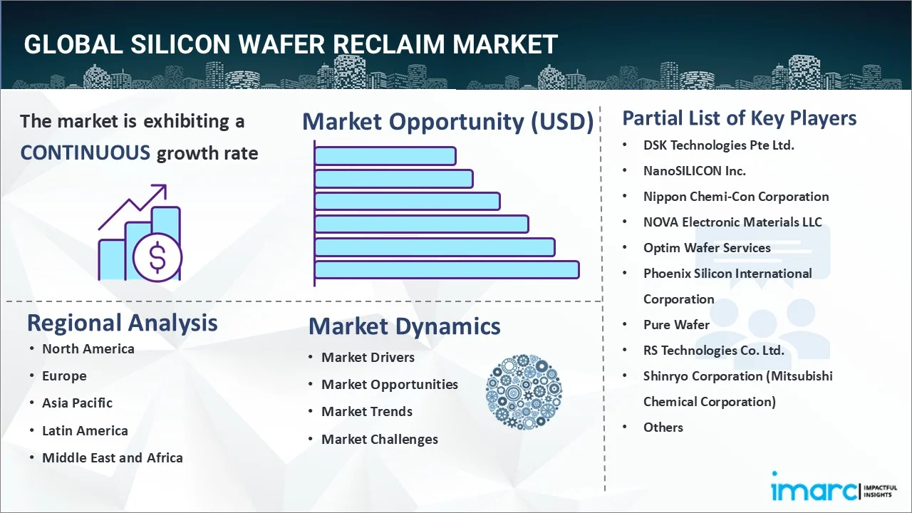
Significant growth in the electronics sector is driving the global market. This can be attributed to the rising demand for smartphones, laptops, and tablets due to its lightweight and recyclable nature. Additionally, the growing focus on solar energy generation and an increase in solar panel installation, supported by government initiatives for renewable energy, are contributing to the market. Governments and international bodies are implementing stricter regulations concerning waste reduction and resource management in tech manufacturing. These policies encourage or even mandate the use of reclaimed materials, thus augmenting the demand for reclaimed silicon wafers. Besides, the increasing consumer awareness about environmental sustainability is pushing companies to adopt greener manufacturing practices. As public interest in eco-friendly products grows, companies have a vested interest in utilizing reclaimed materials, such as silicon wafers, to meet consumer expectations and enhance their brand image. Furthermore, modern technologies, including blockchain and advanced analytics, have made it easier to trace the origin and quality of reclaimed wafers, which in turn is impelling the market.
Silicon Wafer Reclaim Market Trends/Drivers:
Cost-effectiveness
Semiconductor manufacturing is a resource-intensive process that involves the use of high-purity materials, specialized equipment, and substantial energy consumption. Producing new silicon wafers can be expensive, accounting for a sizable portion of the total production cost for semiconductor devices. Reclaimed wafers, on the other hand, can be repurposed at a fraction of the cost, providing substantial cost savings for manufacturers. The economic benefits are even more pronounced for smaller companies and startups in the semiconductor sector, where financial constraints often dictate operational decisions. The ability to reuse wafers allows for a more budget-friendly production cycle, which can result in competitive pricing for the end products. As the global demand for electronic devices continues to soar, manufacturers are under increasing pressure to lower costs while maintaining high-quality standards.
Rising environmental sustainability
The tech industry faces growing scrutiny over its environmental footprint, including the consumption of natural resources and the generation of waste. Silicon wafer reclaim directly addresses these concerns by extending the lifecycle of wafers, thereby reducing the need for new materials. The process of reclaiming wafers involves less energy and fewer raw materials compared to manufacturing new ones, which significantly lowers the overall environmental impact. Numerous organizations are keen to adopt sustainable practices to meet corporate social responsibility goals and adhere to increasingly stringent environmental regulations. The use of reclaimed silicon wafers is not just a cost-saving measure but also an eco-friendly approach that resonates with consumers, stakeholders, and regulatory bodies alike. As sustainability becomes a more critical part of business strategies, the demand for services is expected to rise.
Continual technological advancements
The reclaim process has seen significant improvements in efficiency, precision, and quality control. Advanced techniques now allow for more thorough cleaning, better material recovery, and higher-quality end products. As a result, reclaimed wafers have come closer to matching the performance and reliability of new wafers. This increased quality has helped in broadening the range of applications where reclaimed wafers can be used, thereby expanding the market. Emerging innovations in equipment and process automation have also contributed to faster turnaround times and lower operational costs, making reclaim services even more attractive for manufacturers. As technology continues to advance, it's likely that the capabilities of silicon wafer reclaim will further evolve, thereby reinforcing its position as an essential part of the semiconductor manufacturing landscape.
Silicon Wafer Reclaim Industry Segmentation:
IMARC Group provides an analysis of the key trends in each segment of the market report, along with forecasts at the global, regional, and country levels from 2025-2033. Our report has categorized the market based on diameter type, application and industry vertical.
Breakup by Diameter Type:
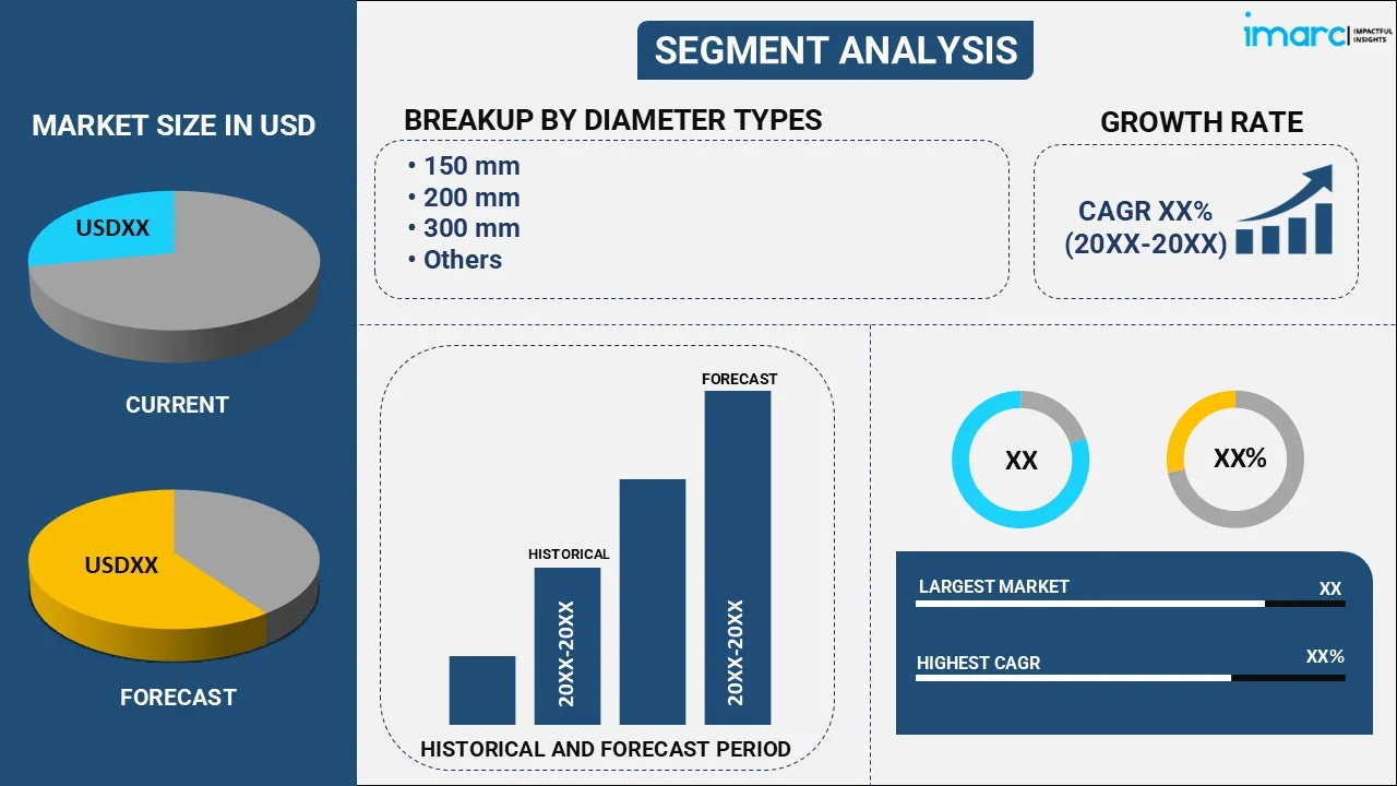
- 150 mm
- 200 mm
- 300 mm
- Others
300mm accounts for the majority of the market share
The report has provided a detailed breakup and analysis of the market based on the diameter type. This includes 150 mm, 200 mm, 300 mm, and others. According to the report, 300 mm represented the largest segment.
300mm wafers offer more surface area compared to smaller diameter wafers, such as 200mm or 150mm. This larger surface area allows to produce more semiconductor devices per wafer, translating to better economies of scale. For semiconductor manufacturers, this means that using 300mm wafers can significantly reduce per-unit production costs, making it a financially appealing option. Moreover, the industry's progression toward smaller and more efficient semiconductor components has made 300mm wafers more compatible with advanced manufacturing technologies. High-performance processors, memory chips, and other cutting-edge semiconductor devices often require the benefits provided by 300mm wafers, such as higher purity and fewer defects, to meet performance and reliability standards. Furthermore, modern reclaim methods can restore these large wafers to near-original condition with high efficiency and minimal waste, making them an attractive choice for manufacturers keen on sustainability.
Breakup by Application:
- Solar Cells
- Integrated Circuits
- Others
Solar cells hold the largest share in the industry
A detailed breakup and analysis of the market based on the application has also been provided in the report. This includes solar cells, integrated circuits, and others. According to the report, solar cells accounted for the largest market share.
Solar energy is increasingly viewed as a viable solution to reduce greenhouse gas emissions and combat climate change. Governments worldwide are providing incentives for the adoption of solar energy, further driving demand for solar cells and, consequently, silicon wafers. Reclaimed wafers offer a cost-effective and sustainable alternative to new wafers, making them an attractive option in large-scale solar energy projects. Additionally, continual technological advancements in the silicon wafer reclaim process have made it possible to produce reclaimed wafers that meet the stringent quality requirements of solar cells. This is crucial as solar cell efficiency is highly dependent on the quality of the silicon wafer. Reclaimed wafers now offer a performance that closely matches that of new wafers, making them more widely acceptable in this application segment. Also, the use of reclaimed silicon wafers in solar cells supports the global shift toward sustainability. The reclaim process minimizes waste and reduces the environmental impact of silicon wafer production, reinforcing the eco-friendly nature of solar energy solutions.
Breakup by Industry Vertical:
- Electronics
- Automotive
- Aerospace and Defense
- Mining and Construction
- Others
Electronics represents the leading market segment
The report has provided a detailed breakup and analysis of the market based on the industry vertical. This includes electronics, automotive, aerospace and defense, mining and construction, and others. According to the report, electronics represented the largest segment.
Devices are becoming smarter, faster, and more energy-efficient, necessitating the use of advanced semiconductor components. Reclaimed silicon wafers offer a cost-effective option for manufacturers to produce high-quality semiconductors, which is especially vital in a market characterized by falling product life cycles and intense competition. Moreover, the quality of reclaimed wafers has improved significantly, du to technological advancements. Modern reclaim processes can produce wafers that meet the rigorous standards required for high-performance electronic devices. This has made reclaimed wafers more appealing for manufacturers in the electronics industry, where quality and reliability cannot be compromised. Also, sustainability is becoming a pivotal concern in the electronics industry, largely due to increasing environmental regulations and consumer demand for eco-friendly products. Using reclaimed silicon wafers aligns with the sustainability objectives of electronic manufacturers and helps them fulfill their corporate social responsibility commitments. This also provides them with a competitive edge in markets where consumers are becoming increasingly eco-conscious.
Breakup by Region:
- North America
- United States
- Canada
- Asia-Pacific
- China
- Japan
- India
- South Korea
- Australia
- Indonesia
- Others
- Europe
- Germany
- France
- United Kingdom
- Italy
- Spain
- Russia
- Others
- Latin America
- Brazil
- Mexico
- Others
- Middle East and Africa
Asia Pacific leads the market, accounting for the largest silicon wafer reclaim market share
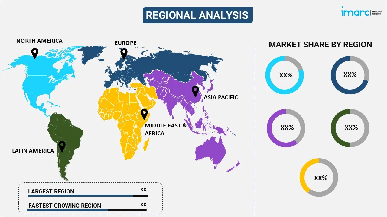
The market research report has also provided a comprehensive analysis of all the major regional markets, which include North America (the United States and Canada); Asia Pacific (China, Japan, India, South Korea, Australia, Indonesia, and others); Europe (Germany, France, the United Kingdom, Italy, Spain, Russia, and others); Latin America (Brazil, Mexico, and others); and the Middle East and Africa. According to the report, Asia Pacific accounted for the largest market share.
Asia Pacific hosts numerous high-tech facilities and semiconductor fabs, which naturally creates a significant demand for silicon wafers. Moreover, the region's focus on innovation and technology adoption provides a conducive environment for the growth of the market. Governments in the Asia Pacific region are heavily investing in R&D and offering incentives to companies that adopt sustainable and technologically advanced practices. This increases the use of reclaimed silicon wafers, which align with both cost-saving and sustainability objectives. Furthermore, rapid industrialization and a growing middle-class population in countries have led to an increased demand for electronic products, from smartphones to home appliances. This increase in consumer demand propels the need for semiconductors and, in turn, silicon wafers. Additionally, the region boasts a robust supply chain and logistics network that facilitates the quick and efficient movement of materials, including reclaimed wafers.
Competitive Landscape:
Several companies aim to produce reclaimed wafers that meet or even exceed the specifications of new wafers. Additionally, several companies are expanding their facilities or forming strategic partnerships to meet the rising demand for reclaimed silicon wafers. This includes mergers, acquisitions, and collaborations with semiconductor manufacturers, research institutions, and technology providers to strengthen their market position. Companies are also focusing on reducing their carbon footprint and waste generation by adopting energy-efficient processes and contributing to circular economy models where wafers can be reused multiple times. Moreover, leading players are continuously working on optimizing operational costs to offer competitive pricing. This includes automating various stages of the reclaim process, improving logistics, and implementing lean manufacturing principles. Companies are further focusing on developing new reclaim techniques, enhancing process efficiencies, and exploring alternative materials that could be reclaimed.
The market research report has provided a comprehensive analysis of the competitive landscape. Detailed profiles of all major companies have also been provided. Some of the key players in the market include:
- DSK Technologies Pte Ltd.
- NanoSILICON Inc.
- Nippon Chemi-Con Corporation
- NOVA Electronic Materials LLC
- Optim Wafer Services
- Phoenix Silicon International Corporation
- Pure Wafer
- RS Technologies Co. Ltd.
- Shinryo Corporation (Mitsubishi Chemical Corporation)
- Silicon Materials Inc.
- Silicon Specialists LLC
- Silicon Valley Microelectronics Inc.
(Please note that this is only a partial list of the key players, and the complete list is provided in the report.)
Recent Developments:
- In September 2022, Silicon Materials Inc. partners With the French Start-Up Novacium to Strengthen Its Innovation Capabilities in New Materials and Processes Critical to Renewable Energy.
- In November 2021, Shinryo Corporation (Mitsubishi Chemical Corporation) announced Expansion of Semiconductor Precision Cleaning Operations. The expansion will feature a new building with an advanced cleanroom, semi-automated chemical cleaning lines, eco-friendly pre-cleaning equipment, and cutting-edge tools for precise semiconductor part cleaning.
- In November 2021, Pure Wafer, a Portfolio Company of Edgewater Capital, Acquires Noel Technologies. Due to this, Pure Wafer enhances its product range with multi-layer and single layer processes, offers high-volume domestic sourcing for standard films, and leverages development capabilities with exotic dielectric and metal films to tap into non-semiconductor markets.
Silicon Wafer Reclaim Market Report Scope:
| Report Features | Details |
|---|---|
| Base Year of the Analysis | 2024 |
| Historical Period | 2019-2024 |
| Forecast Period | 2025-2033 |
| Units | Million USD |
| Scope of the Report | Exploration of Historical Trends and Market Outlook, Industry Catalysts and Challenges, Segment-Wise Historical and Future Market Assessment:
|
| Diameter Types Covered | 150 mm, 200 mm, 300 mm, Others |
| Applications Covered | Solar Cells, Integrated Circuits, Others |
| Industry Verticals Covered | Electronics, Automotive, Aerospace and Defense, Mining and Construction, Others |
| Regions Covered | Asia Pacific, Europe, North America, Latin America, Middle East and Africa |
| Countries Covered | United States, Canada, Germany, France, United Kingdom, Italy, Spain, Russia, China, Japan, India, South Korea, Australia, Indonesia, Brazil, Mexico |
| Companies Covered | DSK Technologies Pte Ltd., NanoSILICON Inc., Nippon Chemi-Con Corporation, NOVA Electronic Materials LLC, Optim Wafer Services, Phoenix Silicon International Corporation, Pure Wafer, RS Technologies Co. Ltd., Shinryo Corporation (Mitsubishi Chemical Corporation), Silicon Materials Inc., Silicon Specialists LLC, Silicon Valley Microelectronics Inc., etc. |
| Customization Scope | 10% Free Customization |
| Post-Sale Analyst Support | 10-12 Weeks |
| Delivery Format | PDF and Excel through Email (We can also provide the editable version of the report in PPT/Word format on special request) |
Key Benefits for Stakeholders:
- IMARC’s industry report offers a comprehensive quantitative analysis of various market segments, historical and current market trends, market forecasts, and dynamics of the silicon wafer reclaim market from 2019-2033.
- The research report provides the latest information on the market drivers, challenges, and opportunities in the global silicon wafer reclaim market.
- The study maps the leading, as well as the fastest-growing, regional markets. It further enables stakeholders to identify the key country-level markets within each region.
- Porter's five forces analysis assist stakeholders in assessing the impact of new entrants, competitive rivalry, supplier power, buyer power, and the threat of substitution. It helps stakeholders to analyze the level of competition within the silicon wafer reclaim industry and its attractiveness.
- Competitive landscape allows stakeholders to understand their competitive environment and provides an insight into the current positions of key players in the market.
Key Questions Answered in This Report
The global silicon wafer reclaim market was valued at USD 617.0 Million in 2024.
We expect the global silicon wafer reclaim market to exhibit a CAGR of 6.34% during 2025-2033.
The increasing application of silicon wafer reclaim in semiconductors and microchips for manufacturing integrated circuits, solar cells, and photoelectric cells, to ensure high operational efficiency, is primarily driving the global silicon wafer reclaim market.
The sudden outbreak of the COVID-19 pandemic had led to the implementation of stringent lockdown regulations across several nations resulting in temporary closure of numerous end-use industries for silicon wafer reclaim.
Based on the diameter type, the global silicon wafer reclaim market can be segmented into 150 mm, 200 mm, 300 mm, and others. Currently, 300 mm holds the majority of the total market share.
Based on the application, the global silicon wafer reclaim market has been divided into solar cells, integrated circuits, and others. Among these, solar cells exhibit a clear dominance in the market.
Based on the industry vertical, the global silicon wafer reclaim market can be categorized into electronics, automotive, aerospace and defense, mining and construction, and others. Currently, the electronics industry accounts for the largest market share.
On a regional level, the market has been classified into North America, Asia-Pacific, Europe, Latin America, and Middle East and Africa, where Asia-Pacific currently dominates the global market.
Some of the major players in the global silicon wafer reclaim market include DSK Technologies Pte Ltd., NanoSILICON Inc., Nippon Chemi-Con Corporation, NOVA Electronic Materials LLC, Optim Wafer Services, Phoenix Silicon International Corporation, Pure Wafer, RS Technologies Co. Ltd., Shinryo Corporation (Mitsubishi Chemical Corporation), Silicon Materials Inc., Silicon Specialists LLC, and Silicon Valley Microelectronics Inc.
Need more help?
- Speak to our experienced analysts for insights on the current market scenarios.
- Include additional segments and countries to customize the report as per your requirement.
- Gain an unparalleled competitive advantage in your domain by understanding how to utilize the report and positively impacting your operations and revenue.
- For further assistance, please connect with our analysts.
 Request Customization
 Speak to an Analyst
 Request Brochure
 Inquire Before Buying



.webp)



.webp)
