Semiconductor Dielectric Etching Equipment Market Report by Type (Wet Etching Equipment, Dry Etching Equipment), Application (Foundries, Integrated Device Manufacturers (IDMs)), and Region 2025-2033
Market Overview:
The global semiconductor dielectric etching equipment market size reached USD 1.3 Billion in 2024. Looking forward, IMARC Group expects the market to reach USD 1.8 Billion by 2033, exhibiting a growth rate (CAGR) of 3.09% during 2025-2033. The significant expansion in the electronics industry, the rising demand for semiconductors, and the increasing penetration of smart devices represent some of the key factors driving the market.
|
Report Attribute
|
Key Statistics
|
|---|---|
|
Base Year
|
2024
|
|
Forecast Years
|
2025-2033
|
|
Historical Years
|
2019-2024
|
|
Market Size in 2024
|
USD 1.3 Billion |
|
Market Forecast in 2033
|
USD 1.8 Billion |
| Market Growth Rate 2025-2033 | 3.09% |
Semiconductor dielectric etching equipment (SDEE) refers to specialized apparatus that is employed to polish and remove various dielectric substances, such as photo-resist mask, silicon oxide, and silicon nitride, during the semiconductor manufacturing procedure. It includes wet and dry etching equipment, which is used with numerous chemicals. In some instances, carbon monoxide is also utilized in the dielectric etching procedure due to higher profile control. These products help carve out varying physical features, including high aspect ratio (HAR), deep trenches, and large cavities. SDEE offers more precision during operations, automates processes, reduces work hazards, and is easier to dispose.
Semiconductor Dielectric Etching Equipment Market Trends:
The significant expansion in the electronics sector and the increasing purchase of various high-performance consumer electronic products, such as smartphones, tablets, and desktops, represent a major factor driving the market toward growth. This can be further attributed to the ongoing trend of miniaturizing semiconductor circuits, which is facilitating the demand for dielectric etching equipment. Additionally, the recent industrial automation across the globe has prompted original equipment manufacturers (OEMs) to widely use the product to fabricate flat panel display screens and not-and (NAND) flash memory, which is acting as another growth-inducing factor. In line with this, significant technological advancements, such as the developments in the dielectric etching equipment capabilities to optimize the semiconductor production operations, are supporting the market growth. Moreover, the large-scale integration of machine learning (ML), artificial intelligence (AI) capabilities, Internet of Things (IoT), and automotive sensors to offer more precision is favoring the market growth. Furthermore, the continuous development of autonomous vehicles has further intensified the usage of semiconductors in vehicles, which is propelling the market growth. The market is also being driven by the widespread adoption of fin-shaped field effect transistor (FinFET) architecture. Since FinFET design uses dielectric etching as one of the major etching steps in its designing process, this is expected to facilitate the demand for semiconductor dielectric etching equipment. Other factors, such as the recent mergers and acquisitions (M&A) amongst key players, recent innovations to introduce more effective product variants, and extensive research and development (R&D) activities, are creating a positive outlook for the market.
Key Market Segmentation:
IMARC Group provides an analysis of the key trends in each segment of the global semiconductor dielectric etching equipment market, along with forecasts at the global, regional, and country level from 2025-2033. Our report has categorized the market based on type and application.
Type Insights:
- Wet Etching Equipment
- Dry Etching Equipment
The report has also provided a detailed breakup and analysis of the semiconductor dielectric etching equipment market based on the type. This includes wet and dry etching equipment. According to the report, dry etching equipment represented the largest segment.
Application Insights:
- Foundries
- Integrated Device Manufacturers (IDMs)
A detailed breakup and analysis of the semiconductor dielectric etching equipment market based on the application has also been provided in the report. This includes foundries and integrated device manufacturers (IDMs). According to the report, IDMs accounted for the largest market share.
Regional Insights:
- North America
- United States
- Canada
- Asia Pacific
- China
- Japan
- India
- South Korea
- Australia
- Indonesia
- Others
- Europe
- Germany
- France
- United Kingdom
- Italy
- Spain
- Russia
- Others
- Latin America
- Brazil
- Mexico
- Others
- Middle East and Africa
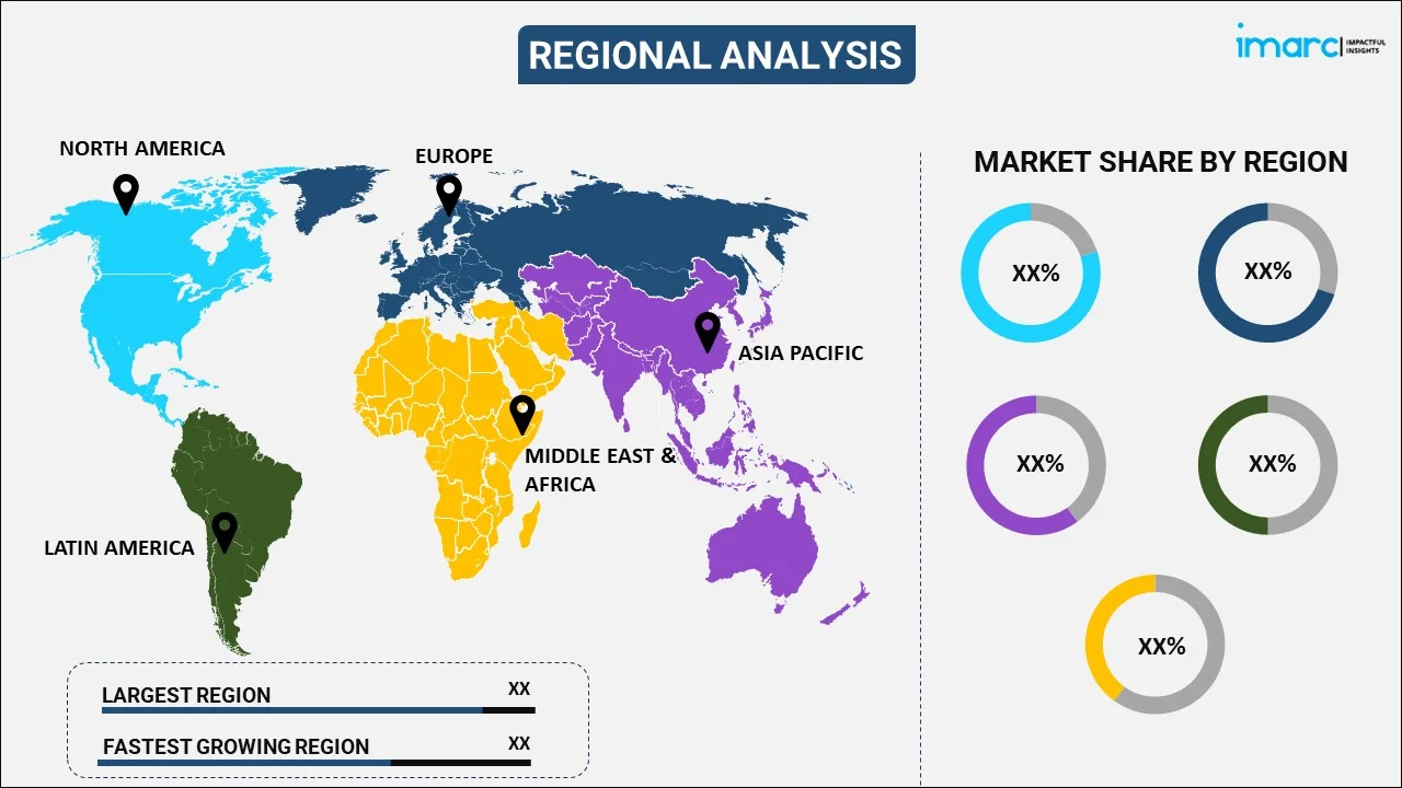
The report has also provided a comprehensive analysis of all the major regional markets that include North America (the United States and Canada); Asia Pacific (China, Japan, India, South Korea, Australia, Indonesia, and others); Europe (Germany, France, the United Kingdom, Italy, Spain, Russia, and others); Latin America (Brazil, Mexico, and others); and the Middle East and Africa. According to the report, Asia Pacific was the largest market for semiconductor dielectric etching equipment. Some of the factors driving the Asia Pacific semiconductor dielectric etching equipment market included extensive research and development (R&D) activities, the increasing demand for smart devices, and significant technological advancements.
Competitive Landscape:
The report has also provided a comprehensive analysis of the competitive landscape in the global semiconductor dielectric etching equipment market. Detailed profiles of all major companies have also been provided. Some of the companies covered include Advanced Micro-Fabrication Equipment Inc. China, Applied Materials Inc., Hitachi High-Technologies Corporation (Hitachi Ltd), Lam Research Corporation, Mattson Technology, Oxford Instruments, SPTS Technologies Ltd. (KLA Corporation), Tokyo Electron Limited, etc. Kindly note that this only represents a partial list of companies, and the complete list has been provided in the report.
Report Coverage:
| Report Features | Details |
|---|---|
| Base Year of the Analysis | 2024 |
| Historical Period | 2019-2024 |
| Forecast Period | 2025-2033 |
| Units | Billion USD |
| Types Covered | Wet Etching Equipment, Dry Etching Equipment |
| Applications Covered | Foundries, Integrated Device Manufacturers (IDMs) |
| Regions Covered | Asia Pacific, Europe, North America, Latin America, Middle East and Africa |
| Countries Covered | United States, Canada, Germany, France, United Kingdom, Italy, Spain, Russia, China, Japan, India, South Korea, Australia, Indonesia, Brazil, Mexico |
| Companies Covered | Advanced Micro-Fabrication Equipment Inc. China, Applied Materials Inc., Hitachi High-Technologies Corporation (Hitachi Ltd), Lam Research Corporation, Mattson Technology, Oxford Instruments, SPTS Technologies Ltd. (KLA Corporation), Tokyo Electron Limited, etc. |
| Customization Scope | 10% Free Customization |
| Post-Sale Analyst Support | 10-12 Weeks |
| Delivery Format | PDF and Excel through Email (We can also provide the editable version of the report in PPT/Word format on special request) |
Key Questions Answered in This Report:
- How has the global semiconductor dielectric etching equipment market performed so far and how will it perform in the coming years?
- What are the drivers, restraints, and opportunities in the global semiconductor dielectric etching equipment market?
- What are the key regional markets?
- Which countries represent the most attractive semiconductor dielectric etching equipment market?
- What is the breakup of the market based on the type?
- What is the breakup of the market based on the application?
- What is the competitive structure of the global semiconductor dielectric etching equipment market?
- Who are the key players/companies in the global semiconductor dielectric etching equipment market?
Key Benefits for Stakeholders:
- IMARC’s report offers a comprehensive quantitative analysis of various market segments, historical and current market trends, market forecasts, and dynamics of the semiconductor dielectric etching equipment market from 2019-2033.
- The research study provides the latest information on the market drivers, challenges, and opportunities in the global semiconductor dielectric etching equipment market.
- The study maps the leading as well as the fastest growing regional markets. It further enables stakeholders to identify the key country-level markets within each region.
- Porter's five forces analysis assist stakeholders in assessing the impact of new entrants, competitive rivalry, supplier power, buyer power, and the threat of substitution. It helps stakeholders to analyze the level of competition within the semiconductor dielectric etching equipment industry and its attractiveness.
- Competitive landscape allows stakeholders to understand their competitive environment and provides an insight into the current positions of key players in the market.
Need more help?
- Speak to our experienced analysts for insights on the current market scenarios.
- Include additional segments and countries to customize the report as per your requirement.
- Gain an unparalleled competitive advantage in your domain by understanding how to utilize the report and positively impacting your operations and revenue.
- For further assistance, please connect with our analysts.
 Request Customization
 Speak to an Analyst
 Request Brochure
 Inquire Before Buying



.webp)



.webp)

