Photomask Market Size, Share, Trends and Forecast by Product, Mask Shop Type, Application, and Region 2026-2034
Photomask Market Size and Share:
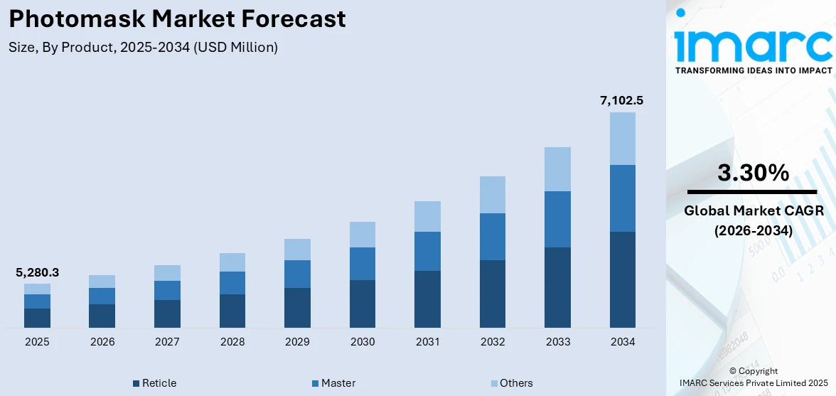
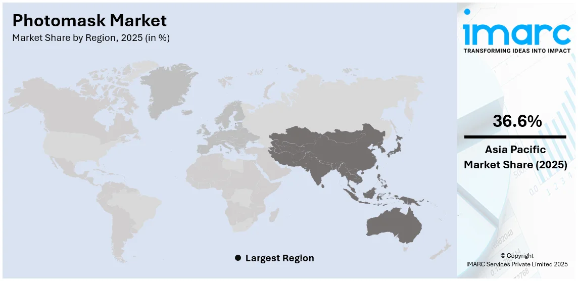
The global photomask market size was valued at USD 5,280.3 Million in 2025. Looking forward, IMARC Group estimates the market to reach USD 7,102.5 Million by 2034, exhibiting a CAGR of 3.30% from 2026-2034. Asia Pacific currently dominates the market, holding a market share of over 36.6% in 2025. The photomask market share is increasing due to the high growth of the semiconductor and integrated circuit electronics and automotive industries, continuing developments in the lithography processes, and innovation on the part of the industry for high-tech devices in the field of semiconductors.
|
Report Attribute
|
Key Statistics
|
|---|---|
|
Base Year
|
2025
|
|
Forecast Years
|
2026-2034
|
|
Historical Years
|
2020-2025
|
| Market Size in 2025 | USD 5,280.3 Million |
| Market Forecast in 2034 | USD 7,102.5 Million |
| Market Growth Rate (2026-2034) | 3.30% |
The photomask market growth is increasing as it plays a crucial role in the semiconductor industry, for the fabrication of integrated circuits (ICs) used in various electronic devices. Photomasks are utilized in photolithography processes to transfer intricate circuit patterns onto semiconductor wafers. With the rapid evolution of semiconductor technologies, the demand for photomasks has surged, driven by advancements in microelectronics, miniaturization of chips, and the growing need for high-performance ICs. Major growth influencers for the photomask market include advanced technologies like 5G, AI, IoT, and autonomous vehicles. Increased consumption of these technologies demands miniaturization and compact semiconductor devices to function properly and sustain themselves for long periods. Thus, these products trigger an increase in the demand for photomasks. The growth is further catalyzed by an increase in semiconductor consumption across diversified industries, which includes automotive, telecommunication, and consumer electronics. Industries will continue to demand higher performance and greater integration of semiconductor devices, while photomasks remain integral to achieving these aims. Their critical role in advancing semiconductor manufacturing processes continues to drive the market, supporting ongoing technological progress in sectors ranging from consumer electronics to automotive and communications.
To get more information on this market Request Sample
The United States emerged as a key regional market for photomasks and is growing rapidly as the semiconductor manufacturing industry remains paramount in the nation's economy.. As one of the largest consumers of advanced semiconductor devices, sectors such as automotive, telecommunication, consumer electronics, and healthcare fuel the demand for photomasks. The United States is a leader in developing these forefront technologies, such as AI, 5G, and autonomous vehicles, which depend on high-performance semiconductors and photomasks by extension. This also assists in boosting further demand for photomasks in the U.S. due to major semiconductor manufacturers such as Intel, TSMC, and Micron. The trend of miniaturization in chip design and the switch to more tightly spaced process nodes are other significant drivers, as these trends require more complex photomasks. The U.S. government's efforts to enhance domestic semiconductor manufacturing create a further expansionary market environment in the photomask industry, as the country seems poised to become the central player in this business.
Photomask Market Trends:
Growing demand for advanced semiconductor devices
The increasing need of advanced semiconductor devices is boosting the photomask demand. This surge is fueled by emerging technologies such as the Internet of Things (IoT), 5G networks, and cloud computing, all of which require more powerful and efficient semiconductor chips. According to a report by the U.S. According to the Department of Commerce, the sale of semiconductors in the United States grew 29% in 2021. The reason is a robust demand for high-performance chips used for everything from smartphone and laptop technology to automotive electronics and industrial machinery. When faster, smaller, and more reliable chips are pushed for in applications, photomasks ensure semiconductor fabrication that's precise and efficient. The need for semiconductor devices further escalates through the trend of adopting AI, edge computing, and connected devices to push photomask manufacturers toward innovation in accordance with the changing nature of market demands. Simultaneously, higher penetration of 5G infrastructure with high data traffic further adds up as a demand for high-performance chips. This exponential demand for advanced devices will continue to play a pivotal role in expanding the photomask market, especially as semiconductor technology moves toward smaller nodes and more intricate chip designs.
Rapid growth of electronics and automotive industries
The electronics and automobile industries are gaining significant momentum. This has directly affected the demand for semiconductors and photomasks. The global electronics industry is experiencing tremendous growth based on the reasons of technological progress, consumer's increased demand for electronic products, and IoT and wearable technology usage at large. The International Trade Administration predicts the global electronics industry will exceed the market value of USD 5 Trillion by 2025 and thus brings along a lot of opportunities for semiconductor and, consequently, photomask manufacturers. The impact is also being seen in the automotive sector in the pursuit of electric vehicles and self-driving technologies, where advanced semiconductors are in demand. Connected vehicles, which rely on sensors, infotainment systems, and autonomous capabilities, further intensify the need for more powerful chips. These trends are leading to the development of complex semiconductor solutions that require advanced photomasks for fabrication. As semiconductor technology becomes more integrated into electronics and automotive applications, the photomask market must adapt to meet the needs of these industries. The increased demand for high-performance chips for applications like electric vehicle batteries, ADAS (advanced driver-assistance systems), and infotainment systems is positioning photomask manufacturers to play an even more significant role in the future.
Technological advancements in lithography processes
Technological innovation in lithography processes is shaping the photomask market trends. One of the most significant developments is the incorporation of extreme ultraviolet, or EUV, lithography. EUV lithography represents a critical step in semiconductor fabrication. This technology permits smaller semiconductor features at higher resolutions and thus gives clients such chips to create advanced, high-performance devices. The International Technology Roadmap for Semiconductors reports that the shipment of EUV tools increased by 50% in 2021 compared to 2020. This indicates a rapid shift toward this cutting-edge technology in the industry. The photomask market is directly affected by the jump in the lithography capability as the photomask optimized for EUV applications becomes imperative for making chips on smaller nodes. Adoption of EUV leads to improved chip performance, cost-effectiveness, and the ability to meet the demand for high-density and power-efficient devices. The semiconductor nodes have shrunk to 5 nm and beyond. Hence, photomasks have to cope with increasing design complexity and the level of precision needed for successful lithography. The rapid adoption pace of EUV, coupled with advancements in mask-making technologies, ensures that photomasks will remain a critical part of semiconductor manufacturing, which will further grow the market.
Photomask Industry Segmentation:
IMARC Group provides an analysis of the key trends in each segment of the global photomask market, along with forecasts at the global, regional, and country levels from 2026-2034. The market has been categorized based on product, mask shop type, and application.
Analysis by Product:
- Reticle
- Master
- Others
Master dominates the market since semiconductor production requires precision. In photomask production, master sets rely on techniques such as e-beam lithography or laser writing to replicate complex circuit patterns on semiconductor wafers. These master sets are the basic patterns used in photomasks to be transferred onto wafers during the manufacturing of semiconductors. With accelerating semiconductor technology, especially regarding the development of devices featuring smaller feature sizes with higher resolutions, the requirement for master sets in the photomask industry has increased. They are critical in the fabrication of advanced semiconductor devices, ensuring submicron-sized patterns are accurately produced. As such, the photomask market has experienced growing demand, as master sets remain a vital component in producing high-performance semiconductors for a range of applications, from consumer electronics to medical devices and telecommunications. With ongoing advancement in semiconductor technology, the photomask industry is set for continued growth as master sets are so central to obtaining higher precision and complexity in semiconductor manufacturing.
Analysis by Mask Shop Type:
- Captive
- Merchant
Captive leads the market as it an integral part of the semiconductor manufacturing process and capture the photomask market due to its strategic importance in vertically integrated semiconductor fabs. Companies can control their supply chains better by having their own photomask production facilities close to the manufacturing floor, reducing lead times, and guarding intellectual property. The proximity between the photomask production facility and the semiconductor manufacturing operations creates more flexibility that allows the production of photomasks to coincide with the actual semiconductor manufacturing processes. Captive mask shops would be ideal for large-scale semiconductor manufacturers and integrated device manufacturers, as they have significant production volumes with complex proprietary designs. By managing their own mask-making operations, these companies can streamline their production processes, enhance quality control, and efficiently manage production schedules. Additionally, having in-house mask production allows for faster turnaround times, which is crucial in the competitive and time-sensitive semiconductor market. The ability to customize and rapidly adapt to evolving technological needs further strengthens the role of captive mask shops in the industry. As demand for advanced semiconductors increases, captive mask shops will continue to hold the dominant shelf, providing crucial support to the semiconductor fabrication process to ensure high-quality semiconductor devices.
Analysis by Application:
Access the comprehensive market breakdown Request Sample
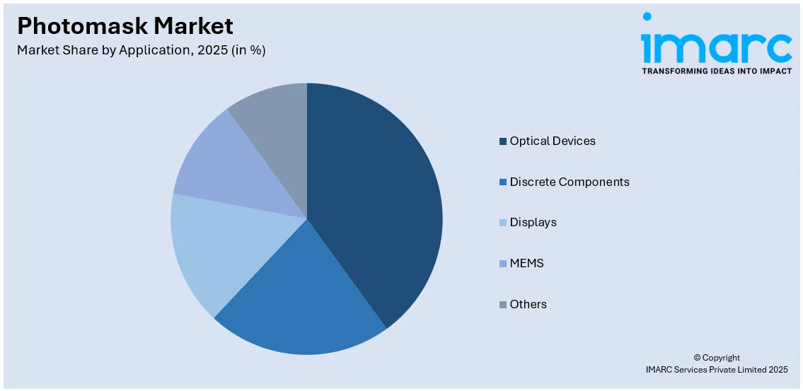
- Optical Devices
- Discrete Components
- Displays
- MEMS
- Others
The optical devices lead the photomask market with a share of 33.0%, mainly due to their crucial role in semiconductor production. Optical devices, including optical aligners and projection aligners, are essential components in photolithography tools used to transfer intricate patterns from photomasks onto semiconductor wafers. As semiconductor technology advances toward smaller feature sizes and higher resolutions, the importance of these optical devices becomes even more pronounced. Optical aligners and projection aligners ensure the accurate and precise transfer of photomask patterns onto substrates, which is crucial for producing modern, high-performance semiconductors. This would call for extremely high precision in photolithography, especially since devices are migrating toward submicron-sized structures. The demands for high-quality optical devices capable of maintaining semiconductor integrity and performance are on the increase. According to the U.S. Bureau of Economic Analysis, the production of optical instruments used in semiconductor manufacturing grew by 8% in the fourth quarter of 2021, reflecting the growing demand for advanced optical technologies. As semiconductor technology is continuously innovating, it can be expected that the reliance of the photomask market on optical devices will grow further, thereby promoting further growth and innovation in the market.
Regional Analysis:
To get more information on the regional analysis of this market Request Sample
- North America
- United States
- Canada
- Asia Pacific
- China
- Japan
- India
- South Korea
- Australia
- Indonesia
- Others
- Europe
- Germany
- France
- United Kingdom
- Italy
- Spain
- Russia
- Others
- Latin America
- Brazil
- Mexico
- Others
- Middle East and Africa
Asia-Pacific dominates the market with a share of 36.6% as the region comprises some of the largest global makers of semiconductors, and this attracts high photomask order placements. Moreover, the region has an electronics sector, which is based in China, South Korea, and Taiwan and is of great importance for the manufacturing of photomasks in semiconductor fabrication. Moreover, it is important to note that the investments in technology and infrastructures that the region makes are the crucial factors that contribute to the growth of the global photomask market. As per the recent figures published by government agencies since 2022, the semiconductor industry in the Asia Pacific region is growing. According to the South Korean Ministry of Trade, exports of the country's semiconductors increased 12% in the first quarter of 2023 from the same period of the year 2022. This is an expansion showing the continuous requirements of photomasks in the Asia Pacific region, thus taking the prime position in the photomask global market.
The North American photomask market is currently growing at a robust rate with the increasing demand for semiconductor devices in consumer electronics, automotive, and telecommunications. The region boasts a strong technological infrastructure, where advanced semiconductor manufacturing facilities support photomask growth. Moreover, the trend toward smaller, yet more powerful, chips for AI, IoT, and 5G applications also fuels demand. Key drivers also include the rise in R&D investments and the presence of major semiconductor players in the U.S., further bolstering market expansion.
Europe’s photomask market is experiencing steady growth, fueled by the region’s emphasis on innovation in semiconductor technologies. The shift toward advanced semiconductor processes, particularly in industries like automotive, healthcare, and industrial automation, is a primary market driver. The high-performance photomask demand is further supported by increased investment in 5G infrastructure and electric vehicles. Besides that, the focus of Europe on maintaining its technological sovereignty regarding the semiconductor sector, strategic initiatives, and collaborations across member states makes the region strong in the global photomask market.
The growth of the photomask market in Latin America is gradually growing due to the growing demand for consumer electronics and the increased production of semiconductors in the region. With the ramp-up in manufacturing capacity by countries such as Brazil and Mexico, the demand for photomasks increases to support the local production of electronic devices. The growth trend in local assembly and manufacturing of automotive and electronics is also another factor involved. Though still emerging, the market will continue growing with the gradual development of technological capabilities and partnerships by regional players to enhance the semiconductor supply chain.
The photomask market for the Middle East and Africa is likely to show growth, helped by investments in infrastructure and technologies. The use of advanced technology is on the rise in areas like telecommunications, energy, and aerospace, propelling the adoption of semiconductors in these sectors. Subsequently, these have led to increased demand for photomasks. The enhanced interest in technology and regional incentives for the technology manufacturing sector fuel growth in this market. However, the growth would be restricted by challenges like the limited facilities of semiconductor manufacturing. This market relies on international collaborations for advanced photomask technology.
Key Regional Takeaways:
United States Photomask Market Analysis
The market is driven by the increasing demand for advanced semiconductor products such as reticles and master photomasks. The demand for smaller, more powerful, and energy-efficient integrated circuits (ICs) is growing across industries like electronics, automotive, and telecommunications. Emerging technologies such as artificial intelligence (AI) and 5G are also driving this growth. For example, as per the IMARC Group, the U.S. AI market was USD 31,807.6 Million in 2023 and is expected to reach USD 97,084.2 Million by 2032 with a CAGR of 12.8% during 2024-2032, indicating a rising need for high-performance semiconductors. Such technologies require precise photomasks for the photolithography process, and advanced reticles and master photomasks are critical to meet this demand. Further stimulating market growth is the U.S. government's investment in semiconductor manufacturing through initiatives like the CHIPS Act, which aims to boost the production capabilities in the country. The automotive industry's shift to electric and autonomous vehicles also fosters the need for specialized photomasks. As industries continue to innovate, the demand for sophisticated photomasks, including reticles and master photomasks, is expected to grow substantially, contributing to the expansion of the U.S. photomask market.
Europe Photomask Market Analysis
The photomask market is driven by increasing demand for advanced semiconductor products, in particular reticles and master photomasks, especially in the automotive and telecommunications industries, and industrial automation. The automotive sector's shift toward electric and self-driving vehicles significantly increases the need for advanced semiconductor chips that are based on high-accuracy photomasks. Furthermore, the region's emphasis on digital transformation, evidenced by industry figures indicating that 29% of EU companies relied on Internet of Things (IoT) devices in 2021, for the most part to secure their premises, makes the demand for advanced electronics move even faster. With increasing adoption of IoT equipment, better performance and power of semiconductors are in demand. This necessitates high-quality reticles and master photomasks for photolithography. Part of the EU's strategy to boost its manufacturing of semiconductors within the region is through such initiatives as the "Digital Compass". As a result, the demand for photomasks, including reticles and masters, is expected to rise, especially as Europe strengthens its technological infrastructure and focuses on sustainability in semiconductor production. These factors collectively suggest robust growth for the photomask market in Europe.
Asia Pacific Photomask Market Analysis
The Asia-Pacific (APAC) photomask market is experiencing robust growth, largely driven by the region's dominance in semiconductor manufacturing. Taiwan, South Korea, and Japan are taking the lead, where demand for advanced reticles and master photomasks for producing state-of-the-art integrated circuits is substantial. Demand is accelerating due to the adoption of newer technologies like 5G, AI, and IoT, where the semiconductor will have to be much smaller and more efficient. For instance, the APAC semiconductor materials market is estimated to grow from USD 40.2 Billion in 2023 to USD 57.0 Billion by 2032, registering a CAGR of 3.84% during 2024-2032. Such growth is mainly due to an increased dependence on high-precision photomasks, especially reticles and master photomasks, in the fabrication of semiconductors. As APAC continues investing in semiconductor innovation and manufacturing capacity, demand for these crucial photomask products will rise, thus expanding the market.
Latin America Photomask Market Analysis
The market for photomasks in Latin America has experienced gradual growth driven by increased reticles and master photomask demand for semiconductors. The consumers' demand in the region increases with respect to consumer electronics, and IoT devices that need sophisticated semiconductor technologies. Moreover, electric vehicle technology from automotive has also accelerated the demand even further. According to industry reports, Latin America saw 184,000 electric vehicles sold in 2024, which contributed to the growing need for advanced chips and, consequently, photomasks. As semiconductor manufacturing capabilities continued to expand, the demand for these products rose.
Middle East and Africa Photomask Market Analysis
In the Middle East and Africa, the market for photomasks is driven by the increasing demand for reticles and master photomasks in this region, particularly in such industries as telecommunications, automotive electronics, and Internet of Things devices. 5G technology is rapidly being adopted as semiconductor needs increase due to the advanced photomasks required for this efficient manufacturing. According to industry reports, by the end of 2026, 5G will account for 73% of all mobile subscriptions in the GCC countries, further driving the demand for high-performance chips. As the region invests in digitalization and expands its manufacturing capabilities, the demand for photomasks is expected to grow.
Competitive Landscape:
Market players in the photomask industry are focusing on enhancing their technological capabilities to meet the growing demand for advanced semiconductor devices. Leaders such as Toppan, Photronics, and Dai Nippon Printing are indeed looking at research and development in order to grow on the photomask side. With semiconductor manufacturers increasingly moving to 7nm, 5nm, and even 3nm technology nodes, photomasks that can support higher process nodes are in increasing demand. This has made a trend for market players to improve photomask manufacturing techniques and enhance mask-making equipment, besides using new materials for performance improvements. Collaboration between photomask manufacturers and semiconductor foundries is also getting more common to respond to specific requirements for next-generation devices. Companies are also reaching out to areas of geographic expansion, with others looking at new growth opportunities within emerging markets in Latin America and the Middle East, where the semiconductor manufacturing process is picking up. The need for specialized photomasks related to automotive, AI, and 5G has led to further diversification by market players for their product line, ensuring greater coverage of areas. These efforts are creating a positive photomask market outlook.
The report provides a comprehensive analysis of the competitive landscape in the photomask market with detailed profiles of all major companies, including:
- Advance Reproductions Corp.
- Applied Materials Inc.
- HOYA Corporation
- Infinite Graphics Incorporated
- KLA Corporation
- LG Innotek Co. Ltd
- Mycronic AB (publ)
- Nippon Filcon Co. Ltd.
- Photronics Inc.
- SK-Electronics Co. Ltd.
- Taiwan Mask Corporation
- Toppan Printing Co. Ltd.
Latest News and Developments:
- October 2024: Toppan Photomask will rename itself Tekscend Photomask Corp. starting November 1, 2024, as it aims to better reflect the advanced microfabrication technology in its products and strengthen global recognition. The name "Tekscend" represents a combination of "technology" and "ascend," the latter signifying the company's commitment to growth and leadership in the semiconductor industry.
- March 2024: Dai Nippon Printing Co., Ltd. (DNP) started full-scale development of photomask manufacturing for 2-nanometer generation logic semiconductors supporting Extreme Ultra-Violet (EUV) lithography. Under this project, DNP was a subcontractor and supplied the newly developed technology to Rapidus Corporation in Tokyo. Rapidus was a participant in the Research and Development Project of the Enhanced Infrastructures for Post-5G Information and Communication Systems, funded by the New Energy and Industrial Technology Development Organization (NEDO).
- Feb 2024: Toppan Photomask partnered with IBM. In a joint effort of mutual strength, they intend to engage in R&D on EUV semiconductor photomasks. It basically aims at consolidating both parties' capabilities and resources to make it more feasible to promote developments for the EMU lithography technology, especially in mask manufacturing, which can produce resolution and quality. This partnership of TPMM and IBM, with deep expertise in photomask manufacturing on the part of TPMM and in semiconductor research on the part of IBM, is eager to address several major problems that EUV lithography has had and advance the next-generation photomask solutions. This contract reflects the interest of both companies in R&D and semiconductor industry development.
- December 2023: Dai Nippon Printing Co., Ltd. (DNP) developed a photomask manufacturing process for 3-nanometer EUV lithography. DNP has a history of innovation, becoming the first to introduce the multi-beam mask writing tool (MBMW) in 2016 and developing photomasks for 5nm EUV in 2020. The latest advancement addresses the semiconductor industry's demand for further miniaturization.
- April 2023: Tokyo-based renowned manufacturer AGC announced plans, at its subsidiary, to raise its production capacity for EUV lithography photomask blanks. AGC is renowned for its expertise in glass, chemicals, and high-tech materials. It did this to meet the growing demands of the semiconductor industry. By expanding the production capacity of EUV lithography photomask blanks, AGC aims to meet the growing demand for cutting-edge solutions in semiconductor manufacturing. The expansion initiative is in line with AGC's strategic vision to strengthen its position as a major provider of essential materials for advanced lithography.
Photomask Market Report Scope:
| Report Features | Details |
|---|---|
| Base Year of the Analysis | 2025 |
| Historical Period | 2020-2025 |
| Forecast Period | 2026-2034 |
| Units | Million USD |
| Scope of the Report |
Exploration of Historical Trends and Market Outlook, Industry Catalysts and Challenges, Segment-Wise Historical and Future Market Assessment:
|
| Products Covered | Reticle, Master, Others |
| Mask Shop Types Covered | Captive, Merchant |
| Applications Covered | Optical Devices, Discrete Components, Displays, MEMS, Others |
| Regions Covered | Asia Pacific, Europe, North America, Latin America, Middle East and Africa |
| Countries Covered | United States, Canada, Germany, France, United Kingdom, Italy, Spain, Russia, China, Japan, India, South Korea, Australia, Indonesia, Brazil, Mexico |
| Companies Covered | Advance Reproductions Corp., Applied Materials Inc., HOYA Corporation, Infinite Graphics Incorporated, KLA Corporation, LG Innotek Co. Ltd, Mycronic AB (publ), Nippon Filcon Co. Ltd., Photronics Inc., SK-Electronics Co. Ltd., Taiwan Mask Corporation, Toppan Printing Co. Ltd. |
| Customization Scope | 10% Free Customization |
| Post-Sale Analyst Support | 10-12 Weeks |
| Delivery Format | PDF and Excel through Email (We can also provide the editable version of the report in PPT/Word format on special request) |
Key Benefits for Stakeholders:
- IMARC’s report offers a comprehensive quantitative analysis of various market segments, historical and current market trends, market forecasts, and dynamics of the photomask market from 2020-2034.
- The research study provides the latest information on the market drivers, challenges, and opportunities in the global photomask market.
- The study maps the leading, and the fastest-growing, regional markets. It further enables stakeholders to identify the key country-level markets within each region.
- Porter's Five Forces analysis assists stakeholders in assessing the impact of new entrants, competitive rivalry, supplier power, buyer power, and the threat of substitution. It helps stakeholders to analyze the level of competition within the photomask industry and its attractiveness.
- Competitive landscape allows stakeholders to understand their competitive environment and provides an insight into the current positions of key players in the market.
Key Questions Answered in This Report
The photomask market was valued at USD 5,280.3 Million in 2025.
The photomask market is estimated to exhibit a CAGR of 3.30% during 2026-2034.
The photomask market is driven by the high growth of the semiconductor and integrated circuit electronics and automotive industries, continuing developments in the lithography processes, and innovation on the part of the industry for high-tech devices in the field of semiconductors.
Asia Pacific currently dominates the market as the region comprises some of the largest global makers of semiconductors, and this attracts high photomask order placements.
Some of the major players in the photomask market include Advance Reproductions Corp., Applied Materials Inc., HOYA Corporation, Infinite Graphics Incorporated, KLA Corporation, LG Innotek Co. Ltd, Mycronic AB (publ), Nippon Filcon Co. Ltd., Photronics Inc., SK-Electronics Co. Ltd., Taiwan Mask Corporation, Toppan Printing Co. Ltd., etc.
Need more help?
- Speak to our experienced analysts for insights on the current market scenarios.
- Include additional segments and countries to customize the report as per your requirement.
- Gain an unparalleled competitive advantage in your domain by understanding how to utilize the report and positively impacting your operations and revenue.
- For further assistance, please connect with our analysts.
 Request Customization
 Speak to an Analyst
 Request Brochure
 Inquire Before Buying
Benefits of Customization
- Personalize this research
- Triangulate with your data
- Get data as per your format and definition
- Gain a deeper dive into a specific application, geography, customer, or competitor
- Any level of personalization
Get in Touch With Us
UNITED STATES
Phone: +1-201-971-6302
INDIA
Phone: +91-120-433-0800
UNITED KINGDOM
Phone: +44-753-714-6104
Email: sales@imarcgroup.com
Client Testimonials
.webp)