Photolithography Equipment Market Size, Share, Trends and Forecast by Process, Wavelength, Device Wavelength, Application, End Use, and Region, 2025-2033
Photolithography Equipment Market Size and Share:
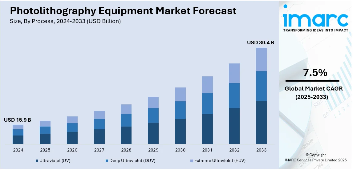
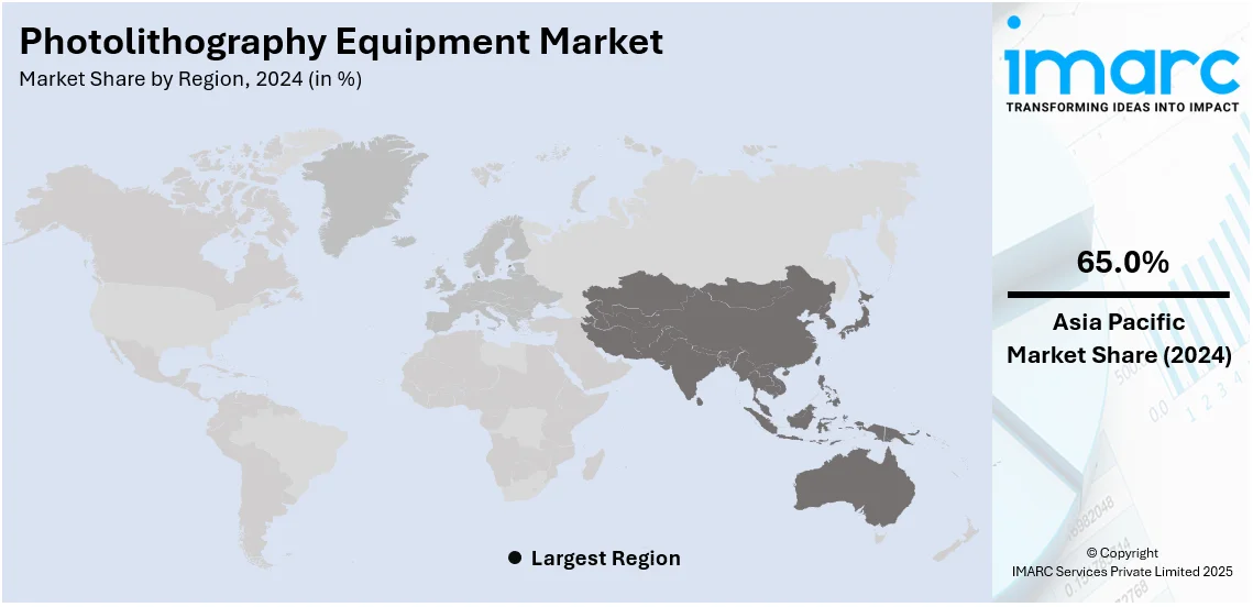
The global photolithography equipment market size was valued at USD 15.9 Billion in 2024. Looking forward, IMARC Group estimates the market to reach USD 30.4 Billion by 2033, exhibiting a CAGR of 7.5% from 2025-2033. Asia Pacific currently dominates the market, holding a market share of over 65.0% in 2024. The Asia Pacific photolithography equipment market share is being driven by the region's leadership in semiconductor production, rising demand for sophisticated electronic devices, and accelerating technology improvements in chip making. High investments in research and development, coupled with growing uptake of 5G and IoT technologies, are also driving the market.
|
Report Attribute
|
Key Statistics
|
|---|---|
|
Base Year
|
2024
|
|
Forecast Years
|
2025-2033
|
|
Historical Years
|
2019-2024
|
|
Market Size in 2024
|
USD 15.9 Billion |
|
Market Forecast in 2033
|
USD 30.4 Billion |
| Market Growth Rate (2025-2033) | 7.5% |
The fast-paced progress in semiconductor technology, especially the need for compact, high-speed, and low-power chips, fuels the market growth of photolithography equipment. The increased demand for high-performance integrated circuits in electronics, automotive, telecom, and consumer electronics industries pushes the use of advanced photolithography equipment. Also, the growth of technologies like 5G, artificial intelligence, and the Internet of Things (IoT) fuels additional demand for advanced semiconductor devices, which need sophisticated photolithography processes. The growing trend towards chip miniaturization to improve performance, lower power consumption, and boost computing power also propels the market. In addition, research and development investments by governments and semiconductor companies greatly contribute to enabling innovation in photolithography equipment, opening new paths for market growth.
To get more information on this market, Request Sample
The United States stands out as a key disruptor in the photolithography equipment market driven by its strong presence in semiconductor manufacturing, cutting-edge research, and technological innovation. Home to major players like Intel, Applied Materials, and Lam Research, the US plays a significant role in advancing photolithography technologies, particularly in areas like extreme ultraviolet (EUV) lithography. The country's ongoing investment in semiconductor R&D, coupled with government initiatives to boost domestic chip production, drives market evolution. Moreover, the rise of emerging technologies such as AI, 5G, and autonomous vehicles, which require increasingly advanced semiconductors, fuels the demand for innovative photolithography equipment. As the US continues to lead in semiconductor manufacturing, its influence on the global photolithography equipment market will remain transformative, pushing for continuous advancements and reshaping industry dynamics.
Photolithography Equipment Market Trends:
Advancements in Extreme Ultraviolet (EUV) lithography
A significant factor providing a positive photolithography equipment market outlook is the rise of extreme ultraviolet (EUV) lithography. EUV technology uses shorter wavelengths of light to create smaller features on semiconductor chips, enabling the production of more powerful and energy-efficient microchips. As semiconductor manufacturers push for smaller nodes and higher performance, EUV has become crucial for the fabrication of advanced integrated circuits, particularly at 7nm and below. This trend is driven by the growing demand for high-performance processors used in AI, 5G, and high-performance computing. Leading photolithography equipment providers, such as ASML, have made substantial investments in EUV technology, which has become central to the production of cutting-edge chips. ASML states that advancements such as EXE, or ‘High NA’, systems represent the newest generation in EUV lithography. Featuring a numerical aperture (NA) of 0.55, their cutting-edge optics deliver enhanced contrast and achieve a print resolution of only 8 nm. The EXE platform is set to facilitate large-scale chip production in 2025–2026, allowing for geometric chip advancements into the next decade. With increasing adoption in major semiconductor fabs worldwide, the transition to EUV lithography is expected to drive significant growth in the market, especially as manufacturers target the 3nm and 2nm nodes in the coming years.
Miniaturization and demand for smaller nodes
The continuous trend of miniaturization in semiconductor production is a key trend in the photolithography equipment industry. Since the need for smaller, quicker, and more efficient electronic components keeps growing, semiconductor producers are working to fabricate chips with progressively smaller nodes, commonly in the 7nm, 5nm, and 3nm range. Smaller nodes make it possible to have more transistors on a piece of real estate, which makes the devices more energy-efficient and performance-driven, as seen in the case of smartphones, laptops, and car electronics. This puts pressure on the photolithography industry to research and come up with more precise and sophisticated machines that can handle these smaller sizes. Smaller and more complex photolithography equipment is necessary in order to keep up with the industry's quest to manufacture high-performance microchips. With semiconductor firms driving node sizes smaller and smaller, the sophisticated photolithography equipment demand will increase, resulting in long-term market expansion.
Adoption of AI and automation in lithography processes
The adoption of artificial intelligence (AI) and automation is another growing trend in the photolithography equipment market. AI technologies are being increasingly integrated into photolithography processes to enhance precision, improve defect detection, and optimize the patterning process. AI-powered tools can analyze vast amounts of data in real-time, allowing for more accurate predictions of performance, improved yield rates, and reduced production costs. Automation is also playing a significant role in improving the efficiency and speed of lithography operations. As semiconductor manufacturing becomes more complex, AI and automation help to reduce human error and the need for manual intervention, ensuring consistent and high-quality outputs. These innovations are especially critical in meeting the demands of advanced semiconductor nodes and the rapid production schedules required for emerging technologies. As the integration of AI and automation continues, the photolithography market is expected to see enhanced productivity and further optimization of semiconductor manufacturing processes.
Photolithography Equipment Industry Segmentation:
IMARC Group provides an analysis of the key trends in each segment of the global photolithography equipment market, along with forecast at the global, regional, and country levels from 2025-2033. The market has been categorized based on process, wavelength, device wavelength, application, and end use.
Analysis by Process:
- Ultraviolet (UV)
- Deep Ultraviolet (DUV)
- Extreme Ultraviolet (EUV)
Ultraviolet stands as the largest component in 2024, holding around 47.5% of the market. Ultraviolet (UV) has emerged as the leading process segment in the photolithography equipment market due to its ability to produce high-resolution patterns on semiconductor wafers. This technology utilizes ultraviolet light to transfer intricate patterns from masks onto silicon wafers, a crucial step in chip production. UV lithography plays a significant role in the fabrication of advanced semiconductor devices, including microprocessors, memory chips, and sensors. As semiconductor manufacturers strive to produce smaller and more powerful chips, UV lithography allows for the creation of fine features at smaller nodes, such as 7nm, 5nm, and beyond. Within this segment, extreme ultraviolet (EUV) lithography is gaining traction for the production of cutting-edge chips, offering even higher precision by using shorter wavelengths of light. The versatility of UV lithography, combined with its cost-effectiveness and scalability, makes it indispensable in semiconductor manufacturing. As the demand for high-performance chips increases, UV lithography will continue to dominate the photolithography equipment market.
Analysis by Wavelength:
- 70 nm–1 nm
- 270 nm–170 nm
- 370 nm–270 nm
70 nm–1 nm stands as the largest component in 2024. The 70 nm–1 nm wavelength segment is a leading range in the photolithography equipment market, driven by the demand for cutting-edge semiconductor manufacturing processes. This wavelength range, particularly in extreme ultraviolet (EUV) lithography, enables the fabrication of semiconductor chips at the smallest nodes, such as 7nm, 5nm, and even down to 1nm. The shorter wavelengths in this range allow for the creation of finer and more precise features on silicon wafers, crucial for producing high-performance microchips used in applications like AI, 5G, and advanced consumer electronics. The 70 nm–1 nm wavelength is particularly important for EUV, where the shorter wavelength improves resolution and ensures the scalability of Moore's Law, enabling continued progress in chip miniaturization. As semiconductor manufacturers continue to push for smaller, more powerful chips, the adoption of photolithography tools utilizing this wavelength segment will remain a key driver of market growth, fueling innovation in semiconductor technology.
Analysis by Device Wavelength:
- Laser Produced Plasmas
- Excimer Lasers
- Mercury Lamps
Laser produced plasmas lead the market share in 2024. Laser-produced plasmas (LPP) are emerging as the leading device wavelength segment in the photolithography equipment market, particularly in the development of extreme ultraviolet (EUV) lithography. LPP technology generates the highly focused, short-wavelength light needed for EUV, which has become crucial for fabricating semiconductor chips at advanced nodes, such as 7nm, 5nm, and below. In LPP systems, a high-powered laser is used to create a plasma from a tin target, emitting EUV light that is then used to pattern semiconductor wafers. This process is essential for producing smaller, more efficient chips used in cutting-edge technologies like 5G, artificial intelligence, and high-performance computing. The precise and high-intensity EUV light produced by LPP systems allows for the intricate patterning required for smaller transistor sizes and complex semiconductor designs. As demand for advanced chips grows, particularly in Asia Pacific and the U.S., LPP-based EUV lithography is expected to continue driving the photolithography equipment market forward.
Analysis by Application:
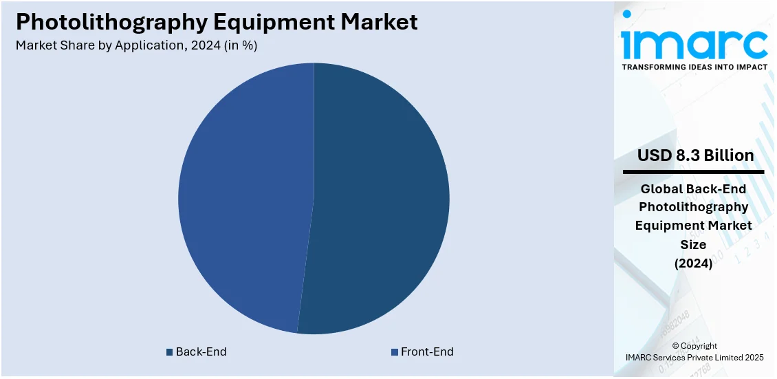
- Front-End
- Back-End
Back-end leads the market with around 52.2% of market share in 2024. The back-end segment is a leading application in the photolithography equipment market, focusing on the final stages of semiconductor manufacturing, where integrated circuits (ICs) are packaged and tested. In this stage, photolithography plays a crucial role in creating precise patterns for the packaging of microchips, ensuring the efficient transfer of signals and power to external components. As demand for smaller, more powerful electronic devices increases, the back-end process requires more advanced photolithography technologies, such as ultra-fine lithography and multi-layer patterning. This trend is driven by the growing need for high-performance chips used in consumer electronics, automotive systems, and telecommunications. The back-end process has become increasingly complex with the miniaturization of chips, which pushes manufacturers to adopt state-of-the-art photolithography equipment for accurate and reliable packaging. Additionally, innovations in advanced packaging techniques, like 3D stacking, further contribute to the growth of the back-end photolithography segment, making it a key driver in the overall market.
Analysis by End Use:
- IDMs
- Foundries
IDMs stands as the largest component in 2024, holding around 56.8% of the market. Integrated Device Manufacturers (IDMs) are the leading end-use segment in the photolithography equipment market, driving significant demand for advanced lithography tools. IDMs, such as Intel, Samsung, and Micron, handle both the design and manufacturing of semiconductor chips, giving them a pivotal role in shaping the industry’s photolithography needs. As these companies push for smaller, more powerful chips to meet the increasing demand for high-performance devices, the need for advanced photolithography equipment, especially extreme ultraviolet (EUV) and deep ultraviolet (DUV) lithography, grows. IDMs are adopting cutting-edge technology to fabricate chips at smaller nodes (e.g., 7nm, 5nm, and 3nm), which require highly precise and sophisticated photolithography processes. Moreover, the increasing push for chips used in emerging technologies such as AI, IoT, and 5G communications further fuels demand for advanced photolithography tools. As a result, IDMs are expected to continue leading the photolithography equipment market, influencing innovation and driving market growth.
Regional Analysis:
- North America
- United States
- Canada
- Asia-Pacific
- China
- Japan
- India
- South Korea
- Australia
- Indonesia
- Others
- Europe
- Germany
- France
- United Kingdom
- Italy
- Spain
- Russia
- Others
- Latin America
- Brazil
- Mexico
- Others
- Middle East and Africa
In 2024, Asia Pacific accounted for the largest market share of over 65.0%. Asia Pacific is the leading regional segment in the photolithography equipment market, driven by the region's dominance in semiconductor manufacturing and technological innovation. Countries like China, Japan, South Korea, and Taiwan are home to major semiconductor giants such as TSMC, Samsung, and SK Hynix, all of which play pivotal roles in global chip production. The region’s strong manufacturing infrastructure and investments in R&D have positioned it as a hub for advanced semiconductor technology. As demand for high-performance chips continues to rise, especially for applications in 5G, artificial intelligence, and consumer electronics, Asia Pacific is expected to maintain its leadership in photolithography equipment adoption. The region's expansion in fabs, particularly for cutting-edge processes like EUV lithography, further fuels market growth. Additionally, government initiatives to bolster semiconductor production and reduce reliance on foreign suppliers are providing strong support to the region's photolithography equipment market, ensuring its dominance in the coming years.
Key Regional Takeaways:
United States Photolithography Equipment Market Analysis
The photolithography equipment market in the United States is primarily driven by advancements in semiconductor technology and increasing demand for high-performance devices. The rapid expansion of the semiconductor industry, particularly in sectors like consumer electronics, automotive, and telecommunications, fuels the need for precision lithography tools. Additionally, the growing adoption of technologies such as artificial intelligence (AI), machine learning, and the Internet of Things (IoT) further accelerates market growth. The U.S. AI market alone is set to reach USD 1,09,514.9 Million by 2033, growing at a CAGR of 12.16% from 2025-2033, reflecting the rising integration of AI in various sectors. Moreover, initiatives like the CHIPS Act are driving domestic semiconductor production, fostering investments in photolithography technologies. The demand for 5G infrastructure and emerging fields like quantum computing also contributes to the need for advanced photolithography equipment. U.S. manufacturers are increasingly adopting extreme ultraviolet (EUV) lithography, which enhances the efficiency of chip production. These factors position the United States as a critical hub for global semiconductor manufacturing, ensuring steady growth for the photolithography equipment market.
Asia Pacific Photolithography Equipment Market Analysis
The photolithography equipment market in APAC is experiencing significant growth, driven by increasing semiconductor demand in industries such as consumer electronics, automotive, and telecommunications. The region's rapid adoption of 5G technology further accelerates this trend. According to GSMA, South Korea had 31.3 Million 5G connections in 2023, accounting for over 48% of all mobile connections, while China recorded more than 700 Million 5G connections, representing 41% of all mobile connections. These developments in mobile connectivity are fueling the demand for advanced semiconductors, which in turn drives the need for high-precision photolithography tools. The ongoing shift toward AI, IoT, and other digital innovations across the region also boosts demand for next-generation chips. Additionally, APAC’s strong semiconductor manufacturing base, with leading countries like Taiwan, South Korea, and China, continues to contribute significantly to the global market, further supporting the growth of photolithography equipment in the region.
Europe Photolithography Equipment Market Analysis
Europe’s photolithography equipment market is witnessing robust growth, driven by the demand for high-performance semiconductors in various industries, including automotive, industrial applications, and consumer electronics. The European Union's focus on digital transformation, green technologies, and innovation fosters significant investments in advanced photolithography solutions. This is further supported by the need for smaller, faster, and more energy-efficient semiconductor devices. Notably, 29% of EU enterprises utilized Internet of Things (IoT) devices in 2021, highlighting the rising integration of connected technologies across industries, which in turn drives the demand for high-precision chips. The automotive industry’s transition to electric vehicles and the growing demand for automation also require advanced semiconductor solutions, boosting photolithography equipment demand. Additionally, the adoption of 5G technology across Europe fuels the need for advanced chips, further propelling the market. The European semiconductor ecosystem benefits from close collaboration between manufacturers, governments, and research institutions, accelerating technological advancements in photolithography processes. Moreover, the European Union’s regulatory framework encourages the development of next-generation semiconductor technologies, creating favorable conditions for photolithography equipment growth. As semiconductor companies expand their production capacities, the demand for advanced photolithography tools, especially extreme ultraviolet (EUV) lithography, is expected to rise, ensuring continued market expansion in the region.
Latin America Photolithography Equipment Market Analysis
Latin America's photolithography equipment market is growing due to rising semiconductor demand across various industries, including automotive and telecommunications. According to GSMA, mobile technologies and services contributed 8% of the region's GDP in 2023, generating USD 520 Billion in economic value, underscoring the importance of digital infrastructure. Governments in Latin America are increasingly investing in technology development, further boosting the demand for advanced semiconductor solutions. The growing adoption of IoT, 5G, and digital transformation initiatives also drives the need for high-performance chips, subsequently increasing the requirement for precise photolithography tools in the region.
Middle East and Africa Photolithography Equipment Market Analysis
The Middle East and Africa market for photolithography equipment is driven by the growth in electronics and telecommunications sectors. The adoption of 5G technology and the increasing demand for smart infrastructure fuel the need for advanced semiconductor devices. The region also saw the deployment of 0.28 Billion Internet of Things (IoT) devices in 2023, further increasing demand for high-precision photolithography tools. As countries in the region expand their digital infrastructure and focus on smart cities, the need for advanced chips grows, pushing the demand for photolithography equipment to new heights.
Competitive Landscape:
Several leading companies in the photolithography equipment market are actively driving growth through continuous technological innovation, strategic partnerships, and investments in research and development (R&D). Major players are leading advancements in photolithography technology, particularly in extreme ultraviolet (EUV) lithography, which is essential for producing chips at smaller nodes like 5nm and below. ASML, for instance, has made substantial strides with its EUV machines, which are critical for semiconductor manufacturers to continue progressing in miniaturization and performance enhancement. These efforts are supported by significant R&D investments aimed at improving the precision and efficiency of photolithography processes, enabling the production of increasingly complex semiconductor devices for applications in AI, 5G, and high-performance computing. Additionally, collaborations between photolithography equipment manufacturers and semiconductor foundries, such as TSMC and Samsung, ensure the development of customized solutions for emerging technologies. Nikon and Canon are also working on advancing their DUV (deep ultraviolet) systems to meet the growing demand for photolithography equipment across various semiconductor nodes. Furthermore, companies are focusing on expanding their global presence, particularly in regions like Asia Pacific, where semiconductor production is booming. These efforts, combined with the pursuit of sustainable manufacturing practices, are fueling the ongoing growth and evolution of the photolithography equipment market.
The report provides a comprehensive analysis of the competitive landscape in the photolithography equipment market with detailed profiles of all major companies, including:
- ASML Holding
- Canon U.S.A., Inc
- Eulitha AG
- Holmarc Opto-Mechatronics Ltd.
- microfab
- Neutronix
- Notion Systems GmbH
- NuFlare Technology Inc.
- S-Cubed
- SUSS MicroTec SE
- Veeco Instruments Inc.
Latest News and Developments:
- December 2024: Canon's India President and CEO, Toshiaki Nomura, stated that the company sees significant opportunities in India for semiconductor lithography equipment. Canon is in discussions with chip manufacturers establishing facilities in the country. Nomura noted that many chip makers are considering India as a new manufacturing hub.
- October 2024: FUJIFILM Corporation has announced the launch of negative-tone resists and developers for EUV lithography, aimed at advancing semiconductor manufacturing. Fujifilm, a pioneer in the NTI process, now offers EUV-compatible resists and developers, enhancing circuit pattern formation and supporting further miniaturization. The company will also expand its production and quality evaluation facilities for these materials at sites in Shizuoka, Japan, and Pyeongtaek, South Korea, with new equipment set to begin operations in October 2025.
- September 2024: FUJIFILM Corporation participated in SEMICON India 2024, held at India Expo Mart, Greater Noida, from September 11 to 13. Fujifilm showcased its semiconductor materials, including photoresists, photolithography materials, CMP slurries, post-CMP cleaners, thin-film chemicals, polyimides, and WAVE CONTROL MOSAIC™ color filter materials for image sensors.
- May 2024: Russia has developed and is testing its first domestically produced photolithography machine for 350nm chips. Deputy Minister Vasily Shpak confirmed this at the CIPR conference, noting that testing is ongoing at the Zelenograd technology production line.
- March 2024: ASML has delivered its 3rd Generation EUV lithography tool, the Twinscan NXE:3800E, featuring a 0.33 numerical aperture lens. This system significantly outperforms the previous NXE:3600D model and is designed for fabricating chips at 3nm, 2nm, and smaller nodes. The NXE:3800E can process over 195 wafers per hour, with a potential throughput upgrade to 220 wph, and offers wafer alignment accuracy of less than 1.1 nm. The tool is now being installed in chip fabs to support the production of advanced chips.
Photolithography Equipment Market Report Scope:
| Report Features | Details |
|---|---|
| Base Year of the Analysis | 2024 |
| Historical Period | 2019-2024 |
| Forecast Period | 2025-2033 |
| Units | Billion USD |
| Scope of the Report |
Exploration of Historical Trends and Market Outlook, Industry Catalysts and Challenges, Segment-Wise Historical and Future Market Assessment:
|
| Processes Covered | Ultraviolet (UV), Deep Ultraviolet (DUV), Extreme Ultraviolet (EUV) |
| Wavelengths Covered | 70 nm–1 nm, 270 nm–170 nm, 370 nm–270 nm |
| Device Wavelengths Covered | Laser Produced Plasmas, Excimer Lasers, Mercury Lamps |
| Applications Covered | Front-End, Back-End |
| End Uses Covered | IDMs, Foundries |
| Regions Covered | Asia Pacific, Europe, North America, Latin America, Middle East and Africa |
| Countries Covered | United States, Canada, Germany, France, United Kingdom, Italy, Spain, Russia, China, Japan, India, South Korea, Australia, Indonesia, Brazil, Mexico |
| Companies Covered | ASML Holding, Canon U.S.A., Inc, Eulitha AG, Holmarc Opto-Mechatronics Ltd., microfab, Neutronix, Notion Systems GmbH, NuFlare Technology Inc., S-Cubed, SUSS MicroTec SE, Veeco Instruments Inc., etc. |
| Customization Scope | 10% Free Customization |
| Post-Sale Analyst Support | 10-12 Weeks |
| Delivery Format | PDF and Excel through Email (We can also provide the editable version of the report in PPT/Word format on special request) |
Key Benefits for Stakeholders:
- IMARC’s report offers a comprehensive quantitative analysis of various market segments, historical and current market trends, market forecasts, and dynamics of the photolithography equipment market from 2019-2033.
- The research study provides the latest information on the market drivers, challenges, and opportunities in the global photolithography equipment market.
- The study maps the leading, as well as the fastest-growing, regional markets. It further enables stakeholders to identify the key country-level markets within each region.
- Porter's Five Forces analysis assists stakeholders in assessing the impact of new entrants, competitive rivalry, supplier power, buyer power, and the threat of substitution. It helps stakeholders to analyze the level of competition within the photolithography equipment industry and its attractiveness.
- Competitive landscape allows stakeholders to understand their competitive environment and provides an insight into the current positions of key players in the market.
Key Questions Answered in This Report
The photolithography equipment market was valued at USD 15.9 Billion in 2024.
The photolithography equipment market is projected to exhibit a CAGR of 7.5% during 2025-2033, reaching a value of USD 30.4 Billion by 2033.
The photolithography equipment market is driven by increasing demand for advanced semiconductors, fueled by applications in AI, 5G, and consumer electronics. Technological advancements, such as EUV lithography, enable smaller, more powerful chips. Additionally, growing investments in semiconductor manufacturing and government initiatives to boost local production further support market growth.
Asia Pacific currently dominates the photolithography equipment market, accounting for a share of 65.0%. The market is driven by strong semiconductor manufacturing growth in countries like Taiwan, South Korea, and Japan, along with the increasing demand for advanced chips in AI, 5G, and consumer electronics.
Some of the major players in the photolithography equipment market include ASML Holding, Canon U.S.A., Inc, Eulitha AG, Holmarc Opto-Mechatronics Ltd., microfab, Neutronix, Notion Systems GmbH, NuFlare Technology Inc., S-Cubed, SUSS MicroTec SE, Veeco Instruments Inc., etc.
Need more help?
- Speak to our experienced analysts for insights on the current market scenarios.
- Include additional segments and countries to customize the report as per your requirement.
- Gain an unparalleled competitive advantage in your domain by understanding how to utilize the report and positively impacting your operations and revenue.
- For further assistance, please connect with our analysts.
 Request Customization
 Speak to an Analyst
 Request Brochure
 Inquire Before Buying
Benefits of Customization
- Personalize this research
- Triangulate with your data
- Get data as per your format and definition
- Gain a deeper dive into a specific application, geography, customer, or competitor
- Any level of personalization
Get in Touch With Us
UNITED STATES
Phone: +1-201-971-6302
INDIA
Phone: +91-120-433-0800
UNITED KINGDOM
Phone: +44-753-714-6104
Email: sales@imarcgroup.com
Client Testimonials

.webp)