Japan Silicon Wafer Market Report by Wafer Size (0 - 100 mm, 100 - 200 mm, 200 - 300 mm, More than 300 mm), Type (N-Type, P-Type), Application (Solar Cells, Integrated Circuits, Photoelectric Cells, and Others), End Use (Consumer Electronics, Automotive, Industrial, Telecommunications, and Others), and Region 2026-2034
Market Overview:
Japan silicon wafer market size reached USD 4.8 Billion in 2025. Looking forward, IMARC Group expects the market to reach USD 6.8 Billion by 2034, exhibiting a growth rate (CAGR) of 4.06% during 2026-2034. The escalating demand for consumer electronics across the globe, the rising support for renewable energy such as solar energy solutions, an increasing demand for smaller and more powerful electronic devices, and the continuous innovations in wafer production techniques represent some of the key factors driving the market.
|
Report Attribute
|
Key Statistics
|
|---|---|
|
Base Year
|
2025 |
|
Forecast Years
|
2026-2034
|
|
Historical Years
|
2020-2025
|
| Market Size in 2025 | USD 4.8 Billion |
| Market Forecast in 2034 | USD 6.8 Billion |
| Market Growth Rate (2026-2034) | 4.06% |
Access the full market insights report Request Sample
A silicon wafer is a thin slice of crystalline silicon which serves as a substrate for the fabrication of semiconductors, an essential component in modern electronics. It is predominantly used in the manufacturing of integrated circuits, photovoltaic cells, and other micro-devices. It comes in various diameters, ranging from less than an inch to up to 12 inches. It can be single-crystalline, multi-crystalline, or amorphous, depending on the production method and end-user requirements. Their adaptability can be further refined through a process known as doping, which involves the introduction of impurities into the silicon wafer to modify its electrical properties. One of the primary advantages of using silicon wafers is the provision of a consistent and high-quality platform for intricate electronic circuitry. Some of the other advantages of silicon wafers include their high thermal conductivity, electrical isolation, and resistance to mechanical and chemical damage. These characteristics make them an ideal choice for applications where precision and reliability are paramount.
Japan Silicon Wafer Market Trends:
The market in Japan is majorly driven by the strong demand for consumer electronics, which necessitates the production of high-quality semiconductor components. Japan's strength in precision engineering also extends to the manufacturing of silicon wafers, where consistency, purity, and surface flatness are paramount. Along with this, the nation's robust automotive sector, which is increasingly adopting smart technologies, further bolsters this demand. Another key trend is the support for renewable energy, specifically solar energy solutions, which extensively use photovoltaic cells made from silicon wafers. In addition, the government's commitment to sustainability and reducing carbon emissions is accelerating the adoption of these technologies, thereby directly influencing the market. This focus aligns with the global trend towards environmentally friendly, low-carbon technologies, an area where Japan has shown leadership. Moreover, there's an increasing demand for smaller and more powerful electronic devices, thus emphasizing the need for silicon wafers that are both thin and durable. Apart from this, innovations in wafer production techniques, such as doping to improve electrical properties, are becoming more refined in Japan, making the country a frontrunner in high-quality silicon wafer production. In confluence with this, the emergence of the Internet of Things (IoT) and 5G technologies is setting new benchmarks for semiconductor performance, quality, and miniaturization, for which silicon wafers are integral. Therefore, this is also significantly supporting the market. Furthermore, the commitment to research and development in Japan is providing cutting-edge innovations that meet domestic demand and have the potential for international market penetration.
Japan Silicon Wafer Market Segmentation:
IMARC Group provides an analysis of the key trends in each segment of the market, along with forecasts at the country level for 2026-2034. Our report has categorized the market based on wafer size, type, application, and end use.
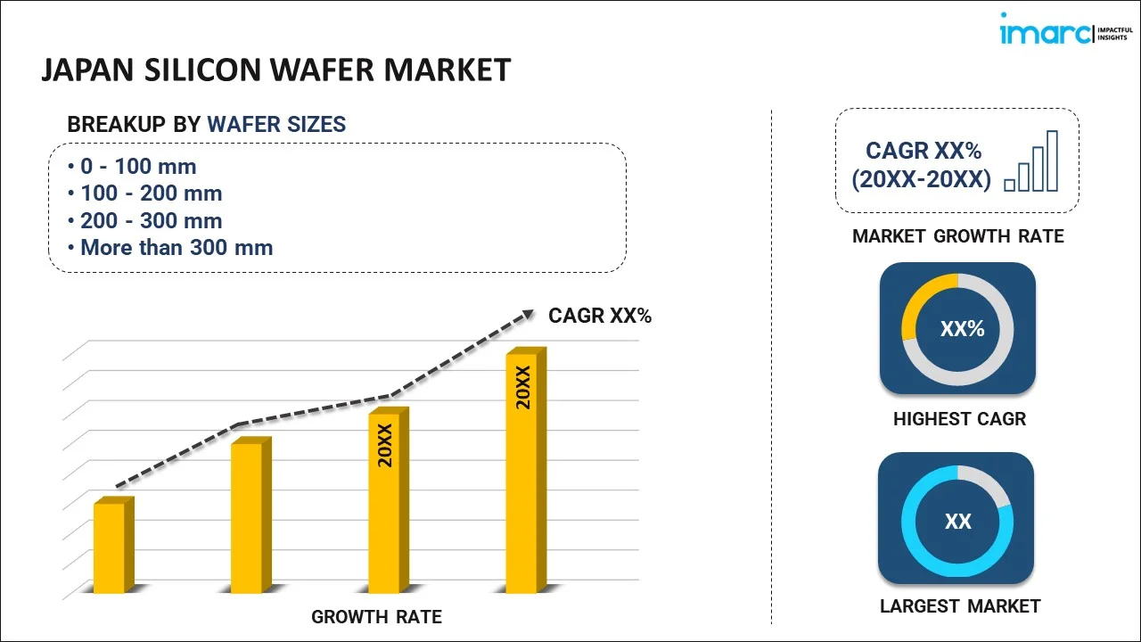
Wafer Size Insights:
To get detailed segment analysis of this market Request Sample
- 0 - 100 mm
- 100 - 200 mm
- 200 - 300 mm
- More than 300 mm
The report has provided a detailed breakup and analysis of the market based on the wafer size. This includes 0 - 100 mm, 100 - 200 mm, 200 - 300 mm, and more than 300 mm.
Type Insights:
- N-Type
- P-Type
A detailed breakup and analysis of the market based on the type have also been provided in the report. This includes N-type and P-type.
Application Insights:
- Solar Cells
- Integrated Circuits
- Photoelectric Cells
- Others
The report has provided a detailed breakup and analysis of the market based on the application. This includes solar cells, integrated circuits, photoelectric cells, and others.
End Use Insights:
- Consumer Electronics
- Automotive
- Industrial
- Telecommunications
- Others
A detailed breakup and analysis of the market based on the end use have also been provided in the report. This includes consumer electronics, automotive, industrial, telecommunications, and others.
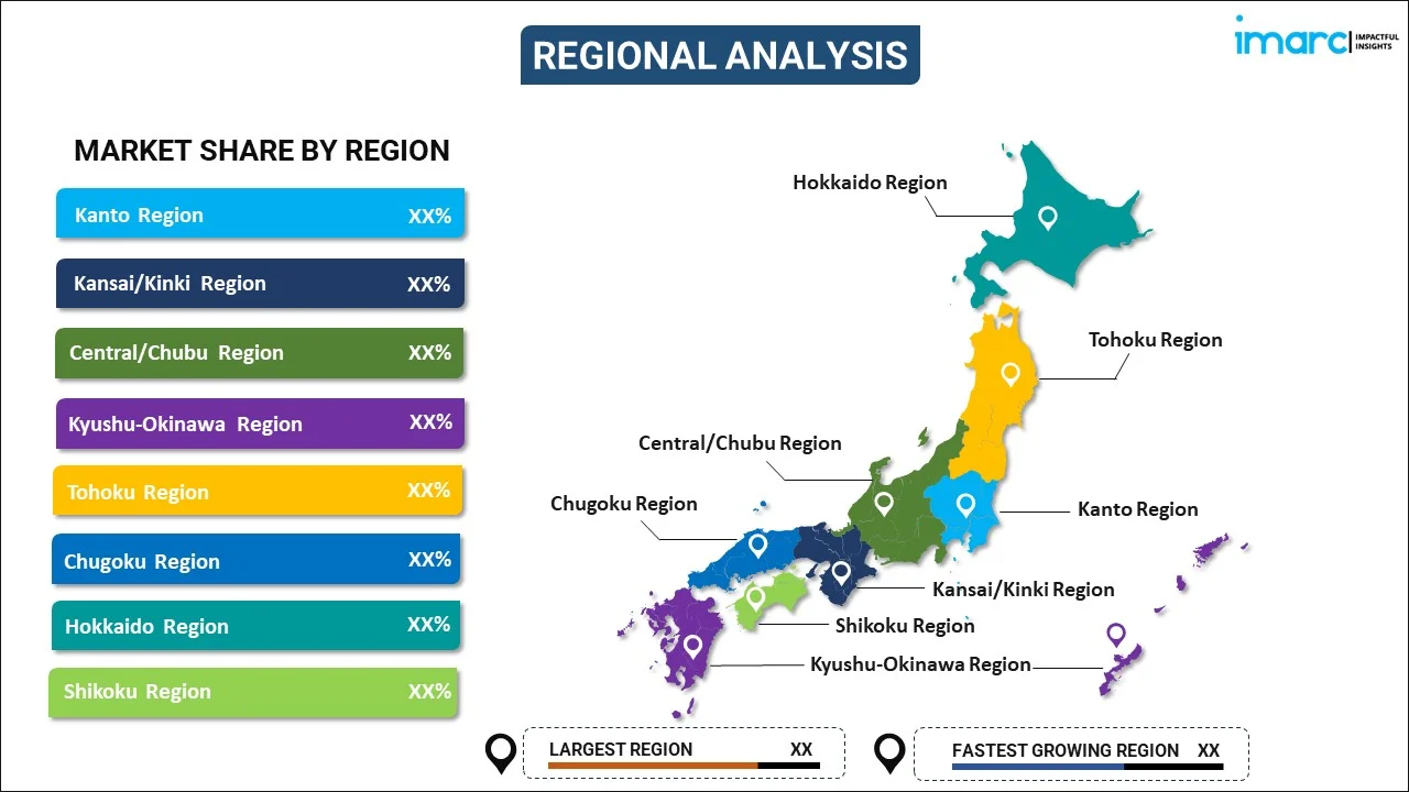
Regional Insights:
To get detailed regional analysis of this market Request Sample
- Kanto Region
- Kansai/Kinki Region
- Central/ Chubu Region
- Kyushu-Okinawa Region
- Tohoku Region
- Chugoku Region
- Hokkaido Region
- Shikoku Region
The report has also provided a comprehensive analysis of all the major regional markets, which include Kanto Region, Kansai/Kinki Region, Central/ Chubu Region, Kyushu-Okinawa Region, Tohoku Region, Chugoku Region, Hokkaido Region, and Shikoku Region.
Competitive Landscape:
The market research report has also provided a comprehensive analysis of the competitive landscape. Competitive analysis such as market structure, key player positioning, top winning strategies, competitive dashboard, and company evaluation quadrant has been covered in the report. Also, detailed profiles of all major companies have been provided.
Japan Silicon Wafer Market Report Coverage:
| Report Features | Details |
|---|---|
| Base Year of the Analysis | 2025 |
| Historical Period | 2020-2025 |
| Forecast Period | 2026-2034 |
| Units | Billion USD |
| Scope of the Report | Exploration of Historical Trends and Market Outlook, Industry Catalysts and Challenges, Segment-Wise Historical and Future Market Assessment:
|
| Wafer Sizes Covered | 0 - 100 mm, 100 - 200 mm, 200 - 300 mm, More than 300 mm |
| Types Covered | N-Type, P-Type |
| Applications Covered | Solar Cells, Integrated Circuits, Photoelectric Cells, Others |
| End Uses Covered | Consumer Electronics, Automotive, Industrial, Telecommunications, Others |
| Regions Covered | Kanto Region, Kansai/Kinki Region, Central/ Chubu Region, Kyushu-Okinawa Region, Tohoku Region, Chugoku Region, Hokkaido Region, Shikoku Region |
| Customization Scope | 10% Free Customization |
| Post-Sale Analyst Support | 10-12 Weeks |
| Delivery Format | PDF and Excel through Email (We can also provide the editable version of the report in PPT/Word format on special request) |
Key Questions Answered in This Report:
- How has the Japan silicon wafer market performed so far and how will it perform in the coming years?
- What has been the impact of COVID-19 on the Japan silicon wafer market?
- What is the breakup of the Japan silicon wafer market on the basis of wafer size?
- What is the breakup of the Japan silicon wafer market on the basis of type?
- What is the breakup of the Japan silicon wafer market on the basis of application?
- What is the breakup of the Japan silicon wafer market on the basis of end use?
- What are the various stages in the value chain of the Japan silicon wafer market?
- What are the key driving factors and challenges in the Japan silicon wafer?
- What is the structure of the Japan silicon wafer market and who are the key players?
- What is the degree of competition in the Japan silicon wafer market?
Key Benefits for Stakeholders:
- IMARC’s industry report offers a comprehensive quantitative analysis of various market segments, historical and current market trends, market forecasts, and dynamics of the Japan silicon wafer market from 2020-2034.
- The research report provides the latest information on the market drivers, challenges, and opportunities in the Japan silicon wafer market.
- Porter's five forces analysis assist stakeholders in assessing the impact of new entrants, competitive rivalry, supplier power, buyer power, and the threat of substitution. It helps stakeholders to analyze the level of competition within the Japan silicon wafer industry and its attractiveness.
- Competitive landscape allows stakeholders to understand their competitive environment and provides an insight into the current positions of key players in the market.
Need more help?
- Speak to our experienced analysts for insights on the current market scenarios.
- Include additional segments and countries to customize the report as per your requirement.
- Gain an unparalleled competitive advantage in your domain by understanding how to utilize the report and positively impacting your operations and revenue.
- For further assistance, please connect with our analysts.
 Request Customization
 Speak to an Analyst
 Request Brochure
 Inquire Before Buying
Benefits of Customization
- Personalize this research
- Triangulate with your data
- Get data as per your format and definition
- Gain a deeper dive into a specific application, geography, customer, or competitor
- Any level of personalization
Get in Touch With Us
UNITED STATES
Phone: +1-201-971-6302
INDIA
Phone: +91-120-433-0800
UNITED KINGDOM
Phone: +44-753-714-6104
Email: sales@imarcgroup.com
Client Testimonials
.webp)