Epitaxial Wafer Market Size, Share, Trends and Forecast by Type, Wafer Size, Application, Industry Vertical, and Region, 2025-2033
Epitaxial Wafer Market Size and Share:
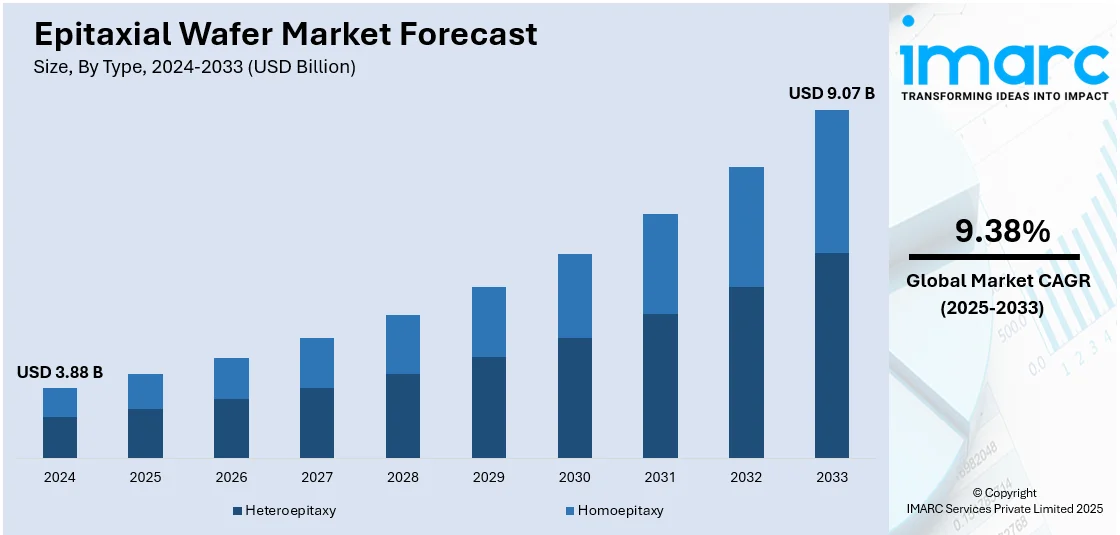
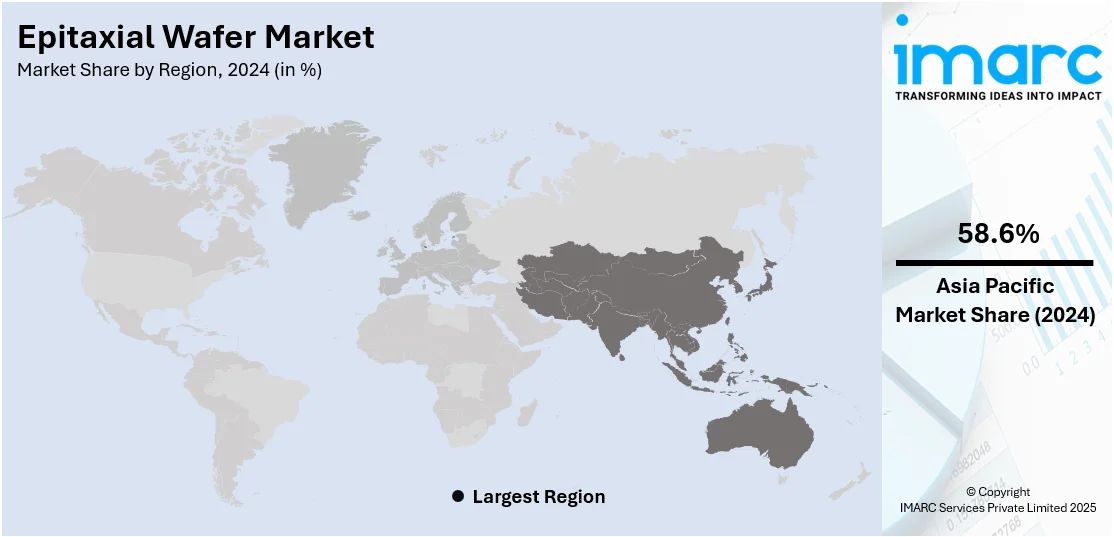
The global epitaxial wafer market size was valued at USD 3.88 Billion in 2024. Looking forward, IMARC Group estimates the market to reach USD 9.07 Billion by 2033, exhibiting a CAGR of 9.38% from 2025-2033. Asia Pacific currently dominates the market, holding a market share of 58.6% in 2024. The market share is expanding, driven by the escalating dependence on high-performance consumer electronics, rising demand for power semiconductor devices and electric vehicles (EVs), and deployment of 5G networks in markets worldwide, creating a need for millimeter-wave and radio frequency (RF) devices.
|
Report Attribute
|
Key Statistics
|
|---|---|
|
Base Year
|
2024
|
|
Forecast Years
|
2025-2033
|
|
Historical Years
|
2019-2024
|
|
Market Size in 2024
|
USD 3.88 Billion |
|
Market Forecast in 2033
|
USD 9.07 Billion |
| Market Growth Rate 2025-2033 | 9.38% |
The market is witnessing robust growth on account of the increasing application across consumer electronics, automotive, and telecommunications industries. With electronic devices shrinking in size, speeding up, and becoming power-efficient, epitaxial wafers are increasingly being used by manufacturers for their better electrical properties and doped profiles. In smartphones and other consumer electronics, these wafers find applications in high-end chipsets and optoelectronic devices, such as light emitting diodes (LEDs) and laser diodes. Within the automotive domain, increasing take-up of electric cars and sophisticated driver-assistance systems (ADAS) further drives the need for power devices produced with the use of epitaxial wafers, particularly silicon carbide (SiC)-based.
The United States epitaxial wafer market is experiencing growth owing to several factors. With strategic efforts towards increasing local chip manufacturing under initiatives, various US-based foundries and fabs are accelerating investment in epitaxial wafer processing. The market is also witnessing increasing momentum from the electric vehicle industry, where silicon carbide (SiC)-based epitaxial wafers play an integral role for effective power management. Besides, the nation's leadership in 5G infrastructure, satellite communications, and defense technologies is catalyzing the demand for compound semiconductor wafers such as gallium arsenide (GaAs) and gallium nitride (GaN). As per the IMARC Group, the US 5G infrastructure market size is expected to exhibit a growth rate (CAGR) of 42.60% during 2024-2032.
Epitaxial Wafer Market Trends:
Rising Demand for High-Performance Consumer Electronics
Consumer electronics manufacturers are focusing on the launch of smaller, faster, and more power-efficient devices. To this end, epitaxial wafers are largely adopted because they have improved electrical properties, such as lower densities of defects and better control of doping profiles. Smartphones, tablets, laptops, smartwatches, and augmented reality (AR) gadgets more and more depend on chips manufactured with epitaxial wafers to achieve performance standards in processing power, battery life, and heat management. Epitaxial layers also make it possible to fit more transistors into small chipsets, a requirement for achieving better computer performance without expanding device size. As new applications are developed, such as foldable phones and artificial intelligence (AI)-enabled devices, the importance of advanced wafers in facilitating high-density, high-performance semiconductor designs becomes increasingly important. In 2024, Huawei released world’s first triple-fold smartphone, the Mate XT. Initially it was exclusively launched in China, later was sold globally.
Expansion of Electric Vehicles (EVs) and Power Electronics
The increasing shift toward electric vehicles (EVs) is substantially catalyzing the demand for power semiconductor devices, most of which are made employing epitaxial wafers, especially those silicon carbide (SiC)-based. These wafers offer high breakdown voltage, low on-resistance, and thermal stability suitable for applications in EVs like inverters, onboard chargers, and power control units. Epitaxial wafers allow manufacturers to create devices that can work at greater voltages and frequencies, making vehicles more efficient and increasing driving range, thereby driving the overall epitaxial wafer market demand. Their application in efficient power supplies and renewable energy devices like solar inverters and wind turbines solidifies their significance in the larger clean energy revolution. Electric car sales stayed strong from the first quarter of 2024, beating those of the same period in 2023 by approximately 25% to reach more than three million. The growing use of wide bandgap semiconductors by the automotive industry highlights the strategic importance of epitaxial wafers in facilitating smaller, more efficient and less failure-prone power modules.
Growing Deployment of 5G Infrastructure and Radio Frequency (RF) Technologies
The deployment of 5G networks in markets worldwide is creating a demand for millimeter-wave and radio frequency (RF) devices, some of which are designed on compound epitaxial substrates like gallium arsenide (GaAs) and gallium nitride (GaN). These semiconductors are critical in the production of high-performance switches, filters, and RF amplifiers that have the capability of meeting the next-generation wireless system's speed and frequency demands. Epitaxial wafers provide greater carrier mobility and power density, key to reducing signal loss and enabling high-speed data transmission on broad bandwidths. Telecommunications gear, base stations, and mobile phones alike take advantage of these characteristics. Moreover, as 5G powers other next-generation technologies such as autonomous systems, Internet of Things (IoT) endpoints, and real-time industrial automation the call for reliable and scalable RF solutions grows louder. The IoT market size is expected to reach USD 3,486.8 Billion by 2033, as per the predictions of the IMARC Group.
Epitaxial Wafer Industry Segmentation:
IMARC Group provides an analysis of the key trends in each segment of the global epitaxial wafer market, along with forecast at the global, regional, and country levels from 2025-2033. The market has been categorized based on type, wafer size, application, and industry vertical.
Analysis by Type:
- Heteroepitaxy
- Homoepitaxy
Heteroepitaxy stands as the largest component, holding 68.7% of the market. It is the process of growing a crystalline layer of one material on the substrate of a different material with a distinct lattice structure. This technique is widely used in semiconductor manufacturing to engineer specific electrical and optical properties that are not achievable with homoepitaxial growth. In heteroepitaxy, materials like gallium arsenide (GaAs), gallium nitride (GaN), or indium phosphide (InP) are grown on silicon or sapphire substrates to produce high-performance devices. Heteroepitaxy is critical for fabricating LEDs, laser diodes, high-electron-mobility transistors (HEMTs), and other optoelectronic or high-speed electronic devices. It allows device designers to combine the favorable properties of multiple materials, leading to performance enhancements across a range of applications.
Analysis by Wafer Size:
- 2-4 Inch
- 5-8 Inch
- 9-12 Inch
- Others
9-12 inch holds the biggest market share. Wafers of these sizes are widely employed in high-end semiconductor manufacturing for the sake of increased production efficiency and reduced cost per chip. The 300 mm (12 inch) wafer is today's industry norm for high-volume production, particularly for logic and memory chips for use in smartphones, servers, and AI accelerators. Bigger wafers enable more chips to be produced per batch, minimizing material waste and overhead costs. Moving to 300 mm and larger also enables tighter process control and better yield for leading-edge nodes. The transition from 200 mm to 300 mm wafers is necessitating heavy investment in compatible manufacturing equipment, but it provides economies of scale essential to contemporary chipmakers.
Analysis by Application:
- LED
- Power Semiconductor
- MEMS-Based Devices
- Others
The LED application segment represents a major use case for epitaxial wafers, particularly those made from gallium nitride (GaN) and gallium arsenide (GaAs), thereby offering a favorable epitaxial wafer market outlook. These materials enable efficient light emission, making them ideal for high-brightness LEDs used in displays, automotive lighting, signage, and general illumination. Epitaxial layers provide precise control over doping and thickness, which are critical for determining the emission wavelength and efficiency of the device.
Power semiconductor devices rely heavily on epitaxial wafers for their capability to manage high voltages, currents, and switching frequencies. Materials like silicon carbide (SiC) and gallium nitride (GaN) are widely used in this segment due to their wide bandgap characteristics, enabling devices to operate at higher temperatures and with better energy efficiency.
Micro-electro-mechanical systems (MEMS) devices incorporate mechanical and electrical components at a microscopic scale and are commonly used in sensors, actuators, and RF switches. Epitaxial wafers play a foundational role in MEMS manufacturing by enabling uniform and high-purity layers needed for precision micromachining. Silicon-based epitaxy is particularly important for creating structures with accurate thickness, doping profiles, and mechanical integrity.
Analysis by Industry Vertical:
- Consumer Electronics
- Automotive
- Healthcare
- Industrial
- Others
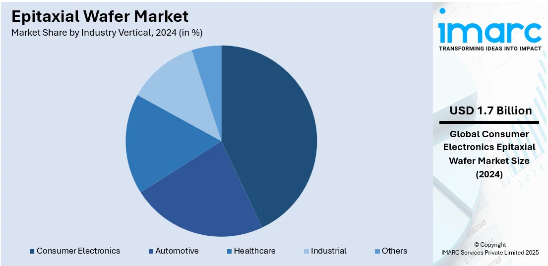
Consumer electronics leads the market with 43.2% of market share in 2024. They remain a leading force behind semiconductor innovation, with increasing demand for faster, smaller, and more power-efficient devices. Smartphones, tablets, laptops, wearable technology, and gaming consoles demand sophisticated chips that provide high processing capabilities while maintaining battery life. Epitaxial wafers play a critical role here, allowing for accurate control of the semiconductor layers employed in producing high-performance integrated circuits. These wafers enable the growth of major components like system-on-chip (SoC) devices, image sensors, and power management ICs. As the market is driven towards 5G-enabled devices, AI-powered features, and high-resolution displays, the demand for secure and scalable chip architectures mounts.
Regional Analysis:
- North America
- United States
- Canada
- Asia Pacific
- China
- Japan
- India
- South Korea
- Australia
- Indonesia
- Others
- Europe
- Germany
- France
- United Kingdom
- Italy
- Spain
- Russia
- Others
- Latin America
- Brazil
- Mexico
- Others
- Middle East and Africa
In 2024, Asia-Pacific accounted for the largest market share of 58.6%. The Asia-Pacific epitaxial wafer market is expanding at a rapid pace driven by the region’s robust semiconductor manufacturing infrastructure and increasing consumer electronics market. Countries are establishing themselves as global leaders in chip production, with large-scale fabs demanding high-quality epitaxial wafers for advanced node technologies. The expansion of 5G infrastructure, increasing demand for EVs, and the shift toward smart manufacturing in the region are further catalyzing the demand for power and RF devices based on epitaxial substrates. Silicon carbide (SiC) and gallium nitride (GaN)-based wafers are also becoming popular because they are well-suited for high-power and high-frequency applications. In addition, government incentives supporting domestic semiconductor capabilities are encouraging new investments in wafer fabrication and material innovation. The presence of key foundries in the region ensures strong local demand, while continued R&D activity contributes to technological improvements in epitaxial wafer quality and scalability.
Key Regional Takeaways:
United States Epitaxial Wafer Market Analysis
The United States hold 88.50% share in North America. The market is primarily driven by rapid advancements in semiconductor technology and the increasing demand for high-performance electronic devices. Epitaxial wafers, essential for manufacturing integrated circuits (ICs) and other semiconductor components, play a vital role in improving the performance, efficiency, and miniaturization of devices such as smartphones, computers, and advanced automotive systems. The expansion of Internet of Things (IoT) applications is also fueling the need for more advanced semiconductor materials, boosting the demand for epitaxial wafers. Additionally, the shift toward electric vehicles (EVs) and renewable energy technologies, which require high-performance semiconductors, has created new opportunities in the market. According to the International Energy Agency, the United States accounted for approximately 10% of all newly registered electric cars in 2023. Furthermore, government investments in the semiconductor industry, including initiatives to boost domestic manufacturing and reduce reliance on foreign suppliers, have increased the development and production of epitaxial wafers. The increasing need for cutting-edge technologies in industries such as aerospace, healthcare, and consumer electronics is also contributing substantially to industry expansion. With a strong focus on innovation and technological progress, the US epitaxial wafer market is poised to continue expanding, driven by the ongoing evolution of the semiconductor industry and the increasing demand for more efficient and powerful electronic systems.
Asia Pacific Epitaxial Wafer Market Analysis
The market is growing due to the rapid expansion of the semiconductor industry, which is critical to the region’s technological advancement. Asia Pacific is a hub for semiconductor manufacturing, requiring various materials such as epitaxial wafers for robust production. As such, the semiconductor materials market in the Asia Pacific region reached USD 41.7 Billion in 2024 and is expected to grow at a CAGR of 3.7% during 2025-2033, as per a report by the IMARC Group. Countries such as China, Japan, South Korea, and Taiwan are leading global production. Additionally, the increasing demand for consumer electronics such as smartphones and wearables, which rely on high-performance semiconductors, has significantly boosted the market for epitaxial wafers. For instance, in India, the smartphone penetration rate reached 46.5% in 2024. Other than this, government initiatives and investments in semiconductor research and development, combined with the strong manufacturing infrastructure in the region, are further fueling industry expansion.
Europe Epitaxial Wafer Market Analysis
The market is experiencing robust growth fueled by the region's focus on advancing semiconductor manufacturing capabilities, particularly in response to the global focus on digital transformation across industries. The EU has also established two primary objectives for the digital transformation of businesses by 2030, requiring over 90% of SMEs to achieve a minimum level of digital intensity and having 75% of EU enterprises utilize artificial intelligence (AI) or cloud computing, according to Eurostat. The growing need for high-speed, high-efficiency devices has also led to an increased demand for advanced semiconductors, with epitaxial wafers playing a crucial role in producing cutting-edge components. Additionally, Europe’s emphasis on developing and deploying autonomous technologies, such as self-driving cars, has driven significant growth in the demand for high-performance chips that require epitaxial wafers. Furthermore, the increasing use of AI and ML in data centers and edge computing applications has heightened the demand for more effective and energy-efficient semiconductors, further boosting the market. Besides this, Europe's growing focus on sustainability and environmental goals has also increased the demand for energy-efficient semiconductors used in green technologies such as electric vehicles (EVs) and renewable energy systems. The combination of these factors, coupled with regional investments in semiconductor innovation, ensures a robust growth trajectory for the European epitaxial wafer market.
Latin America Epitaxial Wafer Market Analysis
The market is significantly influenced by the increasing need for advanced technology in industries such as aerospace, healthcare, and industrial automation. As countries in the region modernize their infrastructure, there is a rising demand for high-performance semiconductors to support the development of smart cities, connected devices, and automation systems. Government initiatives to promote technological advancements, along with an expanding focus on 5G infrastructure, are also contributing substantially to industry expansion. As per recent industry reports, the number of 5G network connections across Latin America reached 67 Million in Q3 2024, recording a growth of 19%. Additionally, the region’s growing interest in data centers and cloud computing technologies is propelling the need for more advanced and efficient semiconductors, supporting overall market growth.
Middle East and Africa Epitaxial Wafer Market Analysis
The market is being propelled by the increasing demand for semiconductors in sectors such as renewable energy and consumer electronics. As the region focuses on sustainable energy solutions, there is a growing need for high-performance semiconductors used in solar power systems and energy-efficient devices. Additionally, the rise of smart technologies, including wearable devices, smart homes, and automation systems, is boosting demand for advanced chips that require epitaxial wafers. The region’s growing focus on digital transformation and smart city development is further increasing the demand for semiconductors. According to the IMARC Group, the Middle East smart cities market is expected to grow at a CAGR of 22.82% during 2025-2033. Besides this, strategic collaborations with global technology companies are further strengthening the market’s growth prospects.
Competitive Landscape:
Market players are actively expanding production capacity, investing in advanced fabrication technologies, and forming strategic partnerships to strengthen their positions. Companies are focusing on improving wafer quality, scaling up 200 mm and 300 mm wafer production, and enhancing capabilities in compound semiconductors like GaN and SiC. Several players are also establishing localized manufacturing units to meet regional demand, especially in Asia-Pacific and North America. Mergers and acquisitions (M&As) are being pursued to gain access to proprietary technologies and broaden product portfolios. Additionally, firms are collaborating with foundries and end-use industries to align product development with the evolving needs of automotive, 5G, and industrial applications, ensuring consistent growth and innovation.
The report provides a comprehensive analysis of the competitive landscape in the epitaxial wafer market with detailed profiles of all major companies, including:
- Electronics And Materials Corporation Limited
- Epistar Corporation
- GlobalWafers (Sino-American Silicon)
- II-VI Incorporated
- IntelliEPI
- IQE PLC
- Jenoptic AG
- Nichia Corporation
- Showa Denko K. K.
- Silicon Valley Microelectronics Inc.
- Siltronic AG (Wacker Chemie AG)
- Sumco Corporation
Latest News and Developments:
- March 2025: Coherent Corporation announced plans to sell its epitaxial fabrication plant located in Champaign, Illinois, as part of its continuous efforts to maximize its production footprint. The facility, spanning 65,000 square feet, houses five G3 epi systems in 15,000 square feet of Class 1000 cleanrooms. The fab formerly manufactured 2-inch to 6-inch indium phosphide and gallium arsenide wafers and can accommodate up to 10 epitaxial tools.
- January 2025: Quintessent Inc, a leading provider of heterogeneous silicon photonics and quantum dot laser technologies, entered a partnership with IQE plc, an industry leader in the epitaxial wafer sector, for the development of the first large-scale semiconductor optical amplifier (SOA) epitaxial wafer supply chain and quantum dot laser in history. With this partnership, IQE will supply Quintessent with a steady supply of epitaxial wafers throughout 2025.
- September 2024: Coherent Corporation, a leading manufacturer of laser technologies, launched its 200 mm silicon carbide epitaxial wafers (SiC epi-wafers). With their advanced thickness and doping homogeneity, the new SiC epi-wafers will enable the manufacturing of exceptional SiC power semiconductors and establish new benchmarks in the industry.
- July 2024: The first Ultra High Vacuum Third-generation Semiconductor Gallium Nitride (GaN) Epitaxial Wafer Pilot Line in Hong Kong was launched during a ceremony organized by MassPhoton Limited and Hong Kong Science and Technology Parks Corporation. This project is a major step forward for the microelectronics sector and a turning point in Hong Kong's transition to new industrialization.
- April 2024: Wolfspeed Inc. selected AIXTRON Tools to aid in the expansion of their 200mm silicon carbide (SiC) epitaxial wafers using AIXTRON’s G10-SiC technologies. AIXTRON’s G10-SiC equipment is an effective and dependable tool that will fulfill the high-volume manufacturing requirements of Wolfspeed Inc., both on their Durham campus and, eventually, at their new 200mm materials.
Epitaxial Wafer Market Report Scope:
| Report Features | Details |
|---|---|
| Base Year of the Analysis | 2024 |
| Historical Period | 2019-2024 |
| Forecast Period | 2025-2033 |
| Units | Billion USD |
| Scope of the Report |
Exploration of Historical Trends and Market Outlook, Industry Catalysts and Challenges, Segment-Wise Historical and Future Market Assessment:
|
| Types Covered | Heteroepitaxy, Homoepitaxy |
| Wafer Sizes Covered | 2-4 Inch, 5-8 Inch, 9-12 Inch, Others |
| Applications Covered | LED, Power Semiconductor, MEMS-Based Devices, Others |
| Industry Verticals Covered | Consumer Electronics, Automotive, Healthcare, Industrial, Others |
| Regions Covered | Asia Pacific, Europe, North America, Latin America, Middle East and Africa |
| Countries Covered | United States, Canada, Germany, France, United Kingdom, Italy, Spain, Russia, China, Japan, India, South Korea, Australia, Indonesia, Brazil, Mexico |
| Companies Covered | Electronics And Materials Corporation Limited, Epistar Corporation, GlobalWafers (Sino-American Silicon), II-VI Incorporated, IntelliEPI, IQE PLC, Jenoptic AG, Nichia Corporation, Showa Denko K. K., Silicon Valley Microelectronics Inc., Siltronic AG (Wacker Chemie AG), Sumco Corporation, etc. |
| Customization Scope | 10% Free Customization |
| Post-Sale Analyst Support | 10-12 Weeks |
| Delivery Format | PDF and Excel through Email (We can also provide the editable version of the report in PPT/Word format on special request) |
Key Benefits for Stakeholders:
- IMARC’s report offers a comprehensive quantitative analysis of various market segments, historical and current market trends, market forecasts, and dynamics of the epitaxial wafer market from 2019-2033.
- The research study provides the latest information on the market drivers, challenges, and opportunities in the global epitaxial wafer market.
- The study maps the leading, as well as the fastest-growing, regional markets. It further enables stakeholders to identify the key country-level markets within each region.
- Porter's Five Forces analysis assists stakeholders in assessing the impact of new entrants, competitive rivalry, supplier power, buyer power, and the threat of substitution. It helps stakeholders to analyze the level of competition within the epitaxial wafer industry and its attractiveness.
- Competitive landscape allows stakeholders to understand their competitive environment and provides an insight into the current positions of key players in the market.
Key Questions Answered in This Report
The epitaxial wafer market was valued at USD 3.88 Billion in 2024.
The epitaxial wafer market is projected to exhibit a CAGR of 9.38% during 2025-2033, reaching a value of USD 9.07 Billion by 2033.
The market is being driven by increasing demand for high-performance consumer electronics, growing adoption of electric vehicles, rising deployment of 5G infrastructure, and the expanding use of power semiconductor devices across multiple industries.
Asia Pacific currently dominates the epitaxial wafer market, accounting for a share of 58.6%. This growth is supported by strong semiconductor manufacturing, rising consumer electronics demand, and regional investments in 5G and electric vehicles.
Some of the major players in the epitaxial wafer market include Electronics And Materials Corporation Limited, Epistar Corporation, GlobalWafers (Sino-American Silicon), II-VI Incorporated, IntelliEPI, IQE PLC, Jenoptic AG, Nichia Corporation, Showa Denko K. K., Silicon Valley Microelectronics Inc., Siltronic AG (Wacker Chemie AG), Sumco Corporation, etc.
Need more help?
- Speak to our experienced analysts for insights on the current market scenarios.
- Include additional segments and countries to customize the report as per your requirement.
- Gain an unparalleled competitive advantage in your domain by understanding how to utilize the report and positively impacting your operations and revenue.
- For further assistance, please connect with our analysts.
 Inquire Before Buying
 Speak to an Analyst
 Request Brochure
 Request Customization
Benefits of Customization
- Personalize this research
- Triangulate with your data
- Get data as per your format and definition
- Gain a deeper dive into a specific application, geography, customer, or competitor
- Any level of personalization
Get in Touch With Us
UNITED STATES
Phone: +1-631-791-1145
INDIA
Phone: +91-120-433-0800
UNITED KINGDOM
Phone: +44-753-714-6104
Email: sales@imarcgroup.com
Client Testimonials

.webp)